Rare earth doped hafnium-based ferroelectric material, preparation method and semiconductor device

A ferroelectric material and rare earth doping technology, applied in semiconductor devices, electric solid devices, electrical components, etc., can solve the problems of weak negative capacitance characteristics of hafnium oxide system, improve the electric domain and inversion speed, and achieve consistent crystal orientation. , fatigue resistance and high reliability

Pending Publication Date: 2019-12-03
INST OF MICROELECTRONICS CHINESE ACAD OF SCI
View PDF5 Cites 3 Cited by
  • Summary
  • Abstract
  • Description
  • Claims
  • Application Information

AI Technical Summary

Problems solved by technology

The battery life of electronic devices using this new type of transistor will be greatly improved. The hafnium-based negative capacitance material is an ideal material for realizing the negative capacitance characteristics of high dielectric metal gates, but the negative capacitance characteristics of the hafnium oxide system are weak, and there is an urgent need for a Materials that can improve the negative capacitance properties of hafnium-based ferroelectric materials

Method used


Image

  • Rare earth doped hafnium-based ferroelectric material, preparation method and semiconductor device
  • Rare earth doped hafnium-based ferroelectric material, preparation method and semiconductor device

Examples


Embodiment Construction

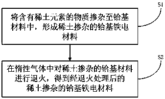
[0034] In order to make the object, technical solution and advantages of the present invention clearer, the present invention will be further described in detail below in conjunction with the accompanying drawings and embodiments. It should be understood that the specific embodiments described here are only used to explain the present invention, not to limit the present invention.

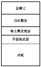
[0035] From the 45nm technology node, the semiconductor industry adopts high dielectric metal gate instead of SiO 2 , under the condition of the same equivalent oxide thickness, the physical thickness of the high-k gate dielectric is increased, so that the leakage current is significantly reduced, and the size of the semiconductor device is further reduced. If a ferroelectric material is added to the gate of the transistor, a negative capacitance value will result. Steering transistors with negative capacitance results in very low power dissipation. The battery life of electronic devices using th...


PUM

PropertyMeasurementUnit
thicknessaaaaaaaaaa
thicknessaaaaaaaaaa
thicknessaaaaaaaaaa

Abstract

The invention provides a rare earth doped hafnium-based ferroelectric material which comprises a hafnium-based ferroelectric material body, rare earth elements are doped in the hafnium-based ferroelectric material body, and the atomic ratio of the doped rare earth elements to hafnium in the hafnium-based ferroelectric material body is (0.1-0.9):1. The invention also provides a preparation method of the rare earth doped hafnium-based ferroelectric material, which comprises the following steps: doping a substance containing rare earth elements into the hafnium-based ferroelectric material to form the rare earth doped hafnium-based ferroelectric material; and annealing the rare earth doped hafnium-based ferroelectric material in inert gas to obtain the annealed rare earth doped hafnium-basedferroelectric material. The invention also provides a semiconductor device. According to the rare earth doped hafnium-based ferroelectric material prepared by the invention, the asymmetry of the material is improved, so that a negative capacitance material can be thinner and has very strong negative capacitance characteristics; and meanwhile, the semiconductor device prepared from the rare earth doped hafnium-based ferroelectric material has very high electric domain and inversion speed, and is higher in fatigue resistance and reliability.

Description

technical field [0001] The invention relates to the field of semiconductors, in particular to a preparation method of a rare earth-doped hafnium-based ferroelectric material and a semiconductor device. Background technique [0002] From the 45nm technology node, the semiconductor industry adopts high dielectric metal gate instead of SiO 2 , under the condition of the same equivalent oxide thickness, the physical thickness of the high-k gate dielectric is increased, so that the leakage current is significantly reduced, and the size of the semiconductor device is further reduced. If a ferroelectric material is added to the gate of the transistor, a negative capacitance value will result. Steering transistors with negative capacitance results in very low power dissipation. The battery life of electronic devices using this new type of transistor will be greatly improved. The hafnium-based negative capacitance material is an ideal material for realizing the negative capacitance...

Claims


Application Information

Patent Timeline
Patent Type & Authority Applications(China)
IPC IPC(8): C23C16/40C23C16/56H01L27/11502
CPCC23C16/405C23C16/40C23C16/56C23C28/042H10B53/00
Inventor 张青竹张兆浩魏千惠屠海令殷华湘魏峰赵鸿滨王文武
Owner INST OF MICROELECTRONICS CHINESE ACAD OF SCI
Why Eureka
Try Eureka