Preparation method of flexible single-layer nano-film memristor

A nano-film and memristor technology, which is applied in the direction of nanotechnology, nanotechnology, nanotechnology for materials and surface science, etc., can solve the problem of memristor materials being hard, commercial production not yet realized, hardware experiments unable to be carried out, etc. question

Active Publication Date: 2016-05-11
SHANDONG UNIV OF SCI & TECH
View PDF5 Cites 6 Cited by
  • Summary
  • Abstract
  • Description
  • Claims
  • Application Information

AI Technical Summary

Problems solved by technology

Most of them adopt the switch model and working mechanism similar to HP memristors, and the manufacturing process is complicated and the cost is high. It is not general and universal for the study of memristor characteristics, memristor circuit theory, and electronic circuit design.
[0006] (2) Commercial production has not yet been realized
[0007] It is difficult for most researchers to obtain a real memristor element, so many researchers cannot carry out hardware experiments in the real physical sense due to the lack of memristor elements when studying memristors and memristor circuits. Rely on simulation or simulated circuits for experimental research
However, the memristor simulation model and the analog circuit are far from the actual memristor characteristics, and the hardware implementation using the analog circuit is more concerned with simulating the memristor mathematical model and ignoring the essential physical characteristics of the memristor
[0008] (3) The preparation of physical memristors that have been reported requires high requirements and harsh conditions in terms of raw material selection and preparation process methods, and it is difficult for laboratories or scientific research units with ordinary conditions to complete the preparation of related physical memristor components.
[0015] 2. The preparation process is complicated, the preparation cycle is long, and the energy consumption is high:
[0017] 3. The material of the prepared memristor is hard and brittle, which is easy to be broken or damaged due to collision, and is not convenient for transportation
[0018] In addition, it also has the problems and deficiencies of relatively harsh process conditions and low product rate.

Method used


Image

  • Preparation method of flexible single-layer nano-film memristor
  • Preparation method of flexible single-layer nano-film memristor
  • Preparation method of flexible single-layer nano-film memristor

Examples


preparation example Construction

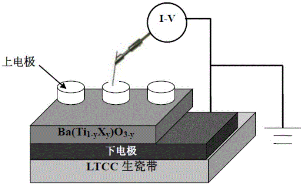
[0145] Adopt the same preparation method of single-layer nanometer film memristor, adopt pulsed laser deposition PLD or magnetron sputtering method to use Au, Ag, Pt to plate electrode, this preparation method comprises the following steps:

[0146] Step 1, with Ba(Ti 1-y x y )O 3-y (X=Mg, Zn, Ca) is used as the target material, and the pulsed laser deposition PLD or magnetron sputtering method is used to coat the LTCC raw ceramic tape with the lower electrode Pt or Au in advance to form a resistive layer. The thickness of the coating is 10-990nm, then heat-treated at 700-900°C for 10-30 minutes;

[0147] In the second step, the target material is Au, Ag or Pt, using pulsed laser method or magnetron sputtering method, in Ba(Ti 1-y x y )O 3-y A layer of upper electrode is plated on the nano film.

[0148] 4, embodiment 22 adopts the Ba(Ti 1-y x y )O 3-y The raw material formula of the mixture target is the same; and, a layer of upper electrode is plated with In-Ga elec...

Embodiment 1

[0155] Preparation of Ba(Ti 1-y x y )O 3-y The raw material formula of the mixture target is: Ba(CH 3 COO) 2 :C 16 h 36 o 4 Ti:X(CH 3 COO) 2 =100:99:1 (molar ratio).

Embodiment 2

[0157] Preparation of Ba(Ti 1-y x y )O 3-y The raw material formula of the mixture target is: Ba(CH 3 COO) 2 :C 16 h 36 o 4 Ti:X(CH 3 COO) 2 =100:98:2 (molar ratio).


PUM

PropertyMeasurementUnit
diameteraaaaaaaaaa
heightaaaaaaaaaa
thicknessaaaaaaaaaa

Abstract

The invention discloses a preparation method of a flexible single-layer nano-film memristor. Holes and ionized oxygen ions generated by the single-layer nano-film memristor under a bias voltage are utilized as charge carriers; and the change principle of the resistance of a device is achieved by change of output of the holes and the ionized oxygen ions, so that a relatively low calcination temperature is combined by omitting a pre-sintering step of a ceramic material of a resistance film and selecting a raw material with a lower nano ceramic sintering temperature from two aspects of simplification of the preapration technology and chemical formulation of the nano ceramic material of the resistance film; B-site substitution is carried out by partially replacing Ti<4+> with X<2+>; the asymmetry of the molecular structure and the hole quantity in the resistance film are increased; by a series of technical means of coating a green tape to form a 'flexible' lower electrode and the like, the preparation technology is simplified; the technological process is shortened; the production efficiency is improved; the production energy consumption and the manufacturing cost are reduced; and the memristive property of the memristor is greatly improved.

Description

technical field [0001] The invention relates to a preparation method of a single-layer nano-film memristor, in particular to a preparation method of a flexible single-layer nano-film memristor; it belongs to the application field of micro-nano electronic devices and nonlinear circuits. Background technique [0002] Memristor (memristor) is the fourth passive circuit component after resistors, capacitors and inductors entered the mainstream electronics field, and it is a passive circuit component related to magnetic flux and charge. As early as 1971, Leon Chua (Cai Shaotang), a pioneer in the theory of international nonlinear circuits and cellular neural networks, theoretically predicted the existence of memristors based on the logical integrity of circuit theory. In 2008, Hewlett-Packard Labs built a memristor prototype device experimentally for the first time, which confirmed Leon Chua's theory about memristors and aroused strong attention worldwide. Memristors have novel ...

Claims


Application Information

Patent Timeline
Patent Type & Authority Applications(China)
IPC IPC(8): H01L45/00B82Y30/00B82Y40/00
CPCB82Y30/00B82Y40/00H10N70/041H10N70/026
Inventor 郭梅窦刚李玉霞李煜于洋孙钊
Owner SHANDONG UNIV OF SCI & TECH
Why Eureka
Try Eureka