Semiconductor packaging test device

A packaging testing and semiconductor technology, applied in the field of semiconductor packaging and testing devices, can solve the problems of affecting detection accuracy, low detection accuracy, low efficiency, etc., and achieve the effect of improving detection accuracy

Inactive Publication Date: 2021-03-19
顺诠达(重庆)电子有限公司
View PDF24 Cites 3 Cited by
  • Summary
  • Abstract
  • Description
  • Claims
  • Application Information

AI Technical Summary

Problems solved by technology

[0003] In order to solve the semiconductor packaging and testing process, for the inspection of the flatness of the packaged chip, the staff needs to put the packaged chip on the inspection table, and then use the CDD camera for overall shooting inspection. The detection accuracy is not high, the efficiency is low, and the inspection table is also easy to fall. Ash also affects the problem of detection accuracy. The purpose of this invention is to provide a semiconductor packaging and testing device

Method used


Image

  • Semiconductor packaging test device
  • Semiconductor packaging test device
  • Semiconductor packaging test device

Examples


Embodiment Construction

[0018] The implementation of the present invention will be illustrated by specific specific examples below, and those skilled in the art can easily understand other advantages and effects of the present invention from the contents disclosed in this specification.

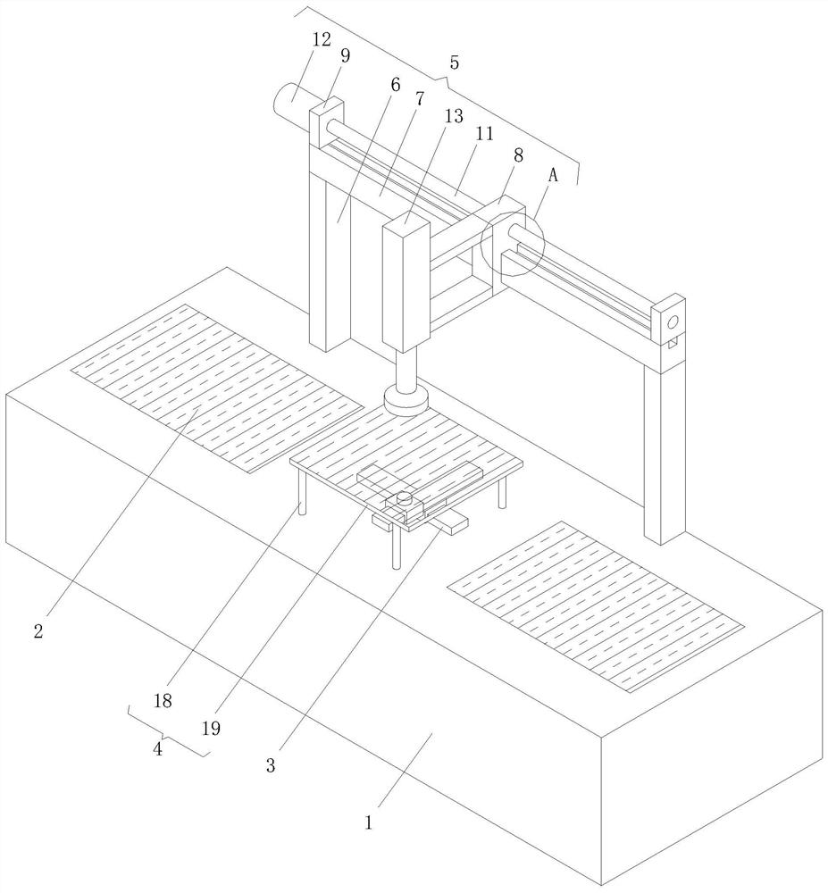
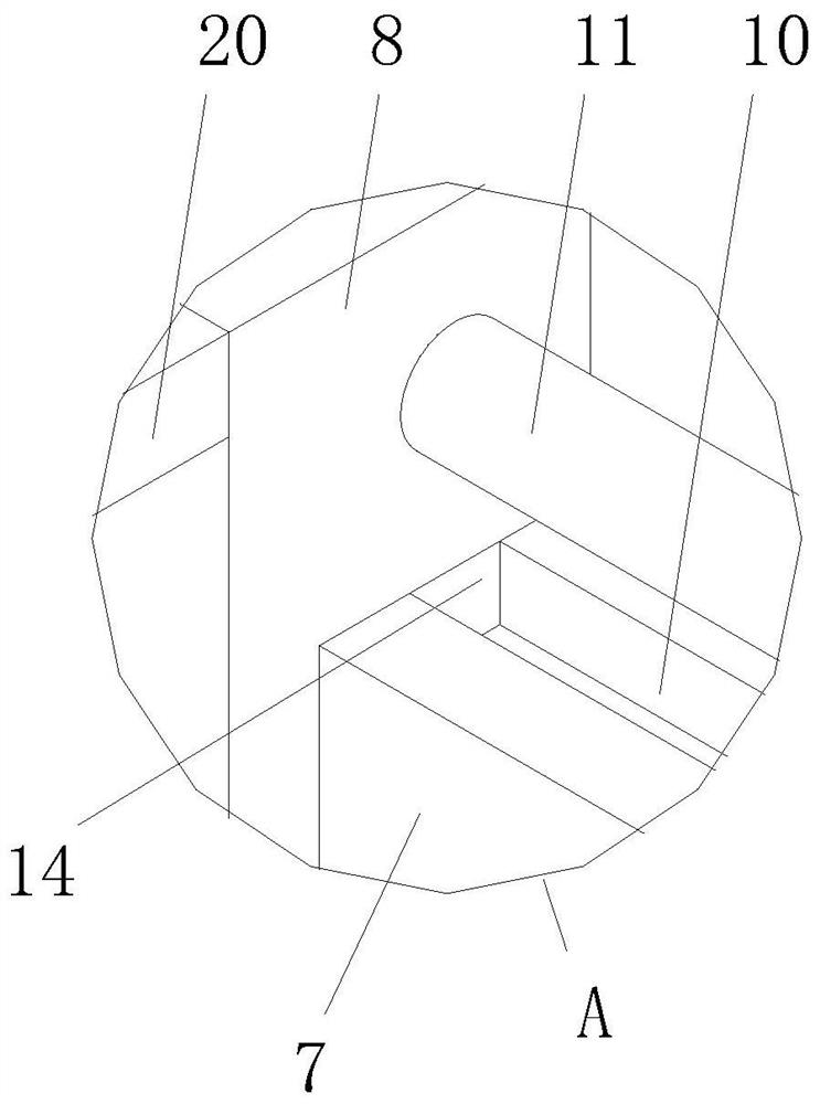
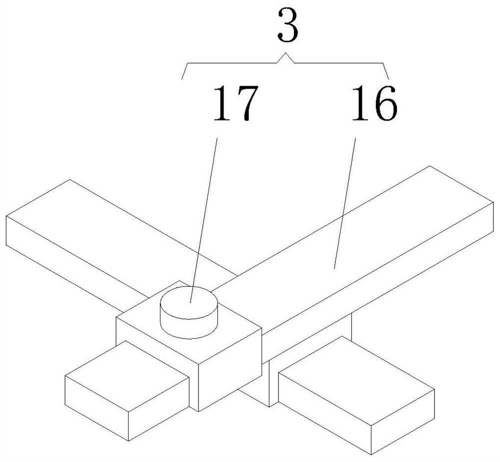
[0019] see Figure 1 to Figure 2 . It should be noted that the structures, proportions, sizes, etc. shown in the drawings in this specification are only used to cooperate with the contents disclosed in the specification, so as to be understood and read by those who are familiar with the technology, and are not used to limit the implementation of the present invention. Restricted conditions, it does not have technical substantive significance, any structural modification, proportional relationship change or size adjustment, without affecting the effect that the present invention can produce and the purpose that can be achieved, should still fall within the present invention. The disclosed technical content must be w...


PUM


Abstract

The invention discloses a semiconductor packaging test device which comprises a platform. The top surface of the platform is provided with two conveyor belts, a packaged chip flatness detection mechanism, a detection table and a transfer mechanism; the transfer mechanism comprises two symmetrically-arranged stand columns, the tops of the stand columns are fixedly connected with a horizontally-arranged sliding rail, the outer wall of the sliding rail is slidably connected with a movable block, the top surface is fixedly connected with two symmetrically-arranged fixing plates, the top surface isprovided with a strip-shaped groove, and a lead screw is rotatably connected to the side walls of the fixing plates in a penetrating mode; and the side wall is fixedly connected with a motor coupledwith the lead screw, and the side wall of the movable block is provided with a material carrying mechanism. The invention relates to the technical field of semiconductor package testing. According tothe invention, the problems of low detection precision, low efficiency, easy ash falling on the detection table and influence on the detection precision due to the fact that a worker needs to place apackaged chip on the detection table and then uses a CDD camera to carry out overall shooting detection in the semiconductor packaging test process for detection of packaged chip flatness are solved.

Description

technical field [0001] The invention relates to the technical field of semiconductor packaging and testing, in particular to a semiconductor packaging and testing device. Background technique [0002] In the prior art, in the semiconductor packaging and testing process, for the inspection of the flatness of the packaged chip, the staff needs to put the packaged chip on the inspection table, and then use the CDD camera for overall shooting inspection, the detection accuracy is not high, and the efficiency is low. At the same time, the inspection table It is also easy to fall dust, which also affects the detection accuracy, so we invented a semiconductor packaging and testing device. Contents of the invention [0003] In order to solve the semiconductor packaging and testing process, for the inspection of the flatness of the packaged chip, the staff needs to put the packaged chip on the inspection table, and then use the CDD camera for overall shooting inspection. The detect...

Claims


Application Information

Patent Timeline
Patent Type & Authority Applications(China)
IPC IPC(8): G01B11/30
CPCG01B11/30
Inventor 游证杰
Owner 顺诠达(重庆)电子有限公司
Why Eureka
Try Eureka