Circuit board chip frame transferring and assembling device and method thereof

An assembly device and frame transfer technology, which is applied to electrical components, electrical components, etc., can solve the problems of low assembly accuracy of chip frame transfer, and achieve the effect of facilitating transfer and grasping, improving grasping accuracy, and preventing movement or shaking.

Inactive Publication Date: 2021-03-19
林佳琳
View PDF1 Cites 0 Cited by
  • Summary
  • Abstract
  • Description
  • Claims
  • Application Information

AI Technical Summary

Problems solved by technology

[0006] The object of the present invention is to solve the above-mentioned problem of low precision of the existing chip frame transfer and assembly, and to provide a circuit board chip frame transfer and assembly device. Mobile positioning accuracy; through the first chip frame clamping module and the second chip frame clamping module, two chip frames can be transferred and assembled at the same time to improve assembly efficiency, and the clamping firmness can be improved through the first chip frame clamping module

Method used


Image

  • Circuit board chip frame transferring and assembling device and method thereof
  • Circuit board chip frame transferring and assembling device and method thereof
  • Circuit board chip frame transferring and assembling device and method thereof

Examples


Embodiment Construction

[0033] The specific implementation manner of the present invention will be described in detail below in conjunction with the accompanying drawings.

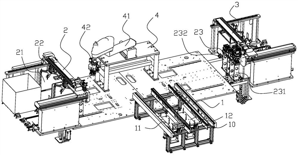
[0034] Such as figure 1 As shown, an automatic assembly and production equipment for circuit board electronic components, the equipment includes a rack and a circuit board feeding positioning device 1 on it, a first chip frame conveying positioning device 2, a second chip frame conveying positioning device 3 and chip Frame transfer assembling device 4; Circuit board feed positioning device 1 comprises circuit board feed support 10, the first circuit board feed assembly 11 and the second circuit board feed assembly 12; Circuit board feed support 10 is arranged on the frame In the middle: the first circuit board feed positioning assembly 11 and the second circuit board feed positioning assembly 12 are arranged in parallel on the circuit board feed support 10; the first circuit board feed positioning assembly 11 and the second circu...


PUM


Abstract

The invention belongs to the technical field of circuit board automatic production, and discloses a circuit board chip frame transferring and assembling device and method. The device comprises a chipframe transfer driving assembly and a chip frame clamping assembly; the chip frame transfer driving assembly is used for driving the chip frame clamping assembly to move and clamp, and assembling thechip frame on the circuit board; the chip frame clamping support plate is arranged on a moving part of the chip frame transfer driving assembly; the first chip frame clamping module and the second chip frame clamping module are arranged on the two sides of the chip frame clamping supporting plate respectively. The chip frame assembly clamping jaw has the advantages that the universality of the chip frame assembly clamping jaw is improved, the accuracy and stability of chip frame assembly clamping are improved, and the automatic assembly efficiency of a circuit board and a chip frame is improved.

Description

technical field [0001] The invention belongs to the technical field of circuit board automatic production, in particular to a circuit board chip frame transfer and assembly device and method thereof. Background technique [0002] In the circuit board production process, it is necessary to install chip frames on the circuit board to facilitate the subsequent installation of chips in their respective chip frames, so that the areas of each chip can be effectively divided and separated, so that each chip can work independently. [0003] Existing circuit board production equipment, such as the Chinese utility model patent application (publication number CN210469919U, announcement date: 20200505), discloses a PCB board assembly mechanism, including a feeding mechanism, a turning mechanism, a shaping mechanism and a feeding mechanism. The board is sent to the turning mechanism, which turns the PCB board over, and the feeding mechanism transports the PCB board from the turning mecha...

Claims


Application Information

Patent Timeline
Patent Type & Authority Applications(China)
IPC IPC(8): H05K13/04H05K13/00
CPCH05K13/0015H05K13/0408H05K13/0417
Inventor 林佳琳朱梅英
Owner 林佳琳
Why Eureka
Try Eureka