A kind of wafer chip cutting method

A cutting method and cutting direction technology, applied in the manufacturing of electrical components, circuits, semiconductor/solid-state devices, etc., can solve the problems of tool damage, chip nicks or cracks, tool collision, etc., to reduce the number of changes and simplify the tool cutting process. Effect

Active Publication Date: 2021-05-14
CHENGDU ADVANCED POWER SEMICON
View PDF4 Cites 0 Cited by
  • Summary
  • Abstract
  • Description
  • Claims
  • Application Information

AI Technical Summary

Problems solved by technology

[0004] The purpose of the present invention is to aim at the existing wafer chip cutting process, especially at the position where the cutter is out of the cutter, the small crystal grains formed in the invalid area of ​​the cutting edge of the cutter are easy to fly away from the blue film and collide with the high-speed rotating cutter when washed by the water flow 1. Injure the tool, the continued processing of the damaged tool will cause gaps or cracks in the chip formed by cutting, and provide a wafer chip cutting method

Method used


Image

  • A kind of wafer chip cutting method
  • A kind of wafer chip cutting method
  • A kind of wafer chip cutting method

Examples


Embodiment 1

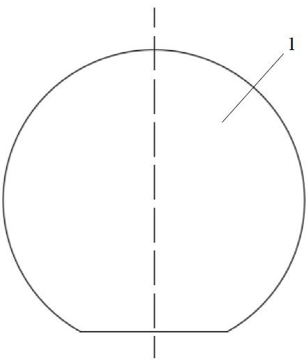
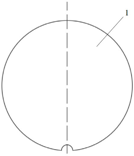
[0033] Such as Figure 6-7 As shown, it is a wafer chip cutting method in this embodiment. After cutting all the first cutting lines 6 in the first cutting direction, the tool cuts all the second cutting lines 7 in the second cutting direction. The cutting direction and the second cutting direction are perpendicular to each other, and the first cutting direction is parallel or perpendicular to the central axis of the wafer chip 1, and at least in the second cutting direction, the cutting position of the cutter is at In the effective area of ​​the wafer chip 1 . Further, the first cutting direction is parallel to the central axis of the wafer chip 1 and is longitudinal, and the second cutting direction is perpendicular to the central axis of the wafer chip 1 and is transverse. In other embodiments, the first cutting direction may be transverse and the second cutting direction may be longitudinal. All of the first cutting lines 6 are parallel to the central axis and adjacent t...

Embodiment 2

[0041] Such as Figure 8 As shown, this embodiment is a wafer chip cutting method, which is different from the cutting method in Embodiment 1 in that the entry position or exit position of all the first dicing lanes 6 is in the second cutting direction Not flush, all close to the edge of the wafer chip 1 . The feeding positions of all the second dicing lines 7 are not flush in the first cutting direction, and are all close to the edge of the wafer chip 1 . Such a design is beneficial to reduce the cutting length of the cutter and consume less time.

Embodiment 3

[0043] This embodiment is a wafer chip cutting method, which is different from the cutting method in Embodiment 1 in that, in the second cutting direction, the cutter is in the same second cutting line 7, first from left to The first cutting is performed on the right, and then the second cutting is performed from right to left. The knife exit positions of the two cuttings are all located at the same position in the effective area. Then the cutter cuts all the second cutting lines 7 one by one. Using the cutting method of this embodiment, although the cutter needs to change direction when cutting the same second cutting line 7, compared with Embodiment 1, the stage carrying the wafer chip 1 does not need to be provided with a driving device to Rotating the wafer chip 1 reduces equipment requirements.


PUM


Abstract

The present invention relates to the technical field of semiconductor manufacturing, in particular to a wafer chip cutting method, in which a tool cuts all the first slits in the first cutting direction and then cuts all the second slits in the second cutting direction. A cutting direction and a second cutting direction are perpendicular to each other, and the first cutting direction is parallel or perpendicular to the central axis of the wafer chip, and at least in the second cutting direction, the cutting position of the cutter is at within the active area of ​​the wafer chip. In the wafer chip cutting method of the present invention, at least in the second cutting direction, the cutting positions of the knives are all in the effective area of ​​the wafer chip, and there is a certain distance from the invalid area of ​​the edge of the wafer chip, which can reduce the existing At the knife exit position, the crystal grains formed in the invalid area of ​​the cutting edge of the knife can easily fly away from the blue film and damage the knife under the impact of the water flow.

Description

technical field [0001] The invention relates to the technical field of semiconductor manufacturing, in particular to a wafer chip cutting method. Background technique [0002] Such as Figure 1-2 As shown, the wafer chip 1 is circular. For positioning, a flat edge (plat) or a V-shaped notch (notch) is usually cut on the wafer chip 1. No matter what type of wafer chip 1 is, there are and only There is a central axis such as Figure 1-2 shown by the dotted line. Such as image 3 As shown, the area of ​​the wafer chip 1 corresponding to a layer of metal layer on the back is called the active area 11 , and the bare silicon area at the edge of the wafer chip 1 is called the edge invalid area 12 . A layer of blue film 2 is pasted on the back of the wafer chip 1 , and the size of the blue film 2 is larger than that of the wafer chip 1 . Because the thickness of the effective area 11 protrudes from the thickness of the edge invalid area 12, the effective area 11 and the blue film...

Claims


Application Information

Patent Timeline
Patent Type & Authority Patents(China)
IPC IPC(8): H01L21/304
CPCH01L21/304
Inventor 刘剑何瑶高忠明
Owner CHENGDU ADVANCED POWER SEMICON
Why Eureka
Try Eureka