Process and device for bonding wafers

a technology of bonding wafers and process, which is applied in the direction of lamination, paper/cardboard containers, containers, etc., can solve the problems of substrate damage, substrate contamination, distortion of the structure of the substrate and/or the m rang

Active Publication Date: 2008-06-26
THALLNER ERICH
View PDF1 Cites 19 Cited by
  • Summary
  • Abstract
  • Description
  • Claims
  • Application Information

AI Technical Summary

Benefits of technology

[0012]The invention is therefore based on the object of proposing an extremely gently operating device and a corresponding process for wafers in which scratches and contamination are as far as possible avoided.
[0015]The basic idea of the present invention is to avoid the disadvantages listed above by constructing the pressure contact surface to the semiconductor substrate or wafer from a softer but heat-resistant material or a material having the same thermal expansion coefficient as the substrates or one of the substrates, in particular wafer or semiconductor substrate.
[0022]When the upper and / or the lower pressure plate are formed from the same base material as the substrate in contact with the particular substrate contact surface, the corresponding pressure plate and the substrate in contact with this expand uniformly when the temperature changes, as a result of which scratches and deposits can be avoided.
[0024]If at least one pressure plate is constructed from plastic, it is advantageous to carry out the charging of the substrates with heat in the device according to the invention at a temperature above 100° C., in particular between 250 and 300° C., preferably at a temperature of between 275 and 285° C., with simultaneous charging with pressure, in particular with a pressure of from 500 N to 80,000 N, and only then to carry out a higher charging with heat of above 300° C., in particular without charging with pressure, in a further device in order to avoid damage to the plastic on the pressure plate in the device according to the invention. The dwell time in the device according to the invention can thus be reduced, and because of the exclusive charging with heat in the further device, contamination and scratching are avoided. The course of the process is accordingly divided over two devices, which leads to a further optimization of the process.

Problems solved by technology

Application of a contact force in combination with changes in temperature (heating up and cooling down) causes impairments and contamination of the substrates.
The substrates are moreover contaminated by metal ions contained in the holding plate and / or pressure plate, since the intensive contact can effect atomic transfer of metal ions to the substrate.
In particular during curing of the optional bonding layer between the wafers under an applied pressure, stresses may be caused in the bonding layer, which can lead to distortions of the structures on the substrate and / or substrates in the μm range.
Because of the scratches and particles, an expensive cleaning (over-etching) following the bonding operation is often necessary, in order to be able to use the substrate further in the process line (in a clean room).
Metal ions can diffuse into the semiconductor crystal during subsequent oven processes and adversely influence properties thereof as a semiconductor.

Method used


Image

  • Process and device for bonding wafers
  • Process and device for bonding wafers

Examples


Embodiment Construction

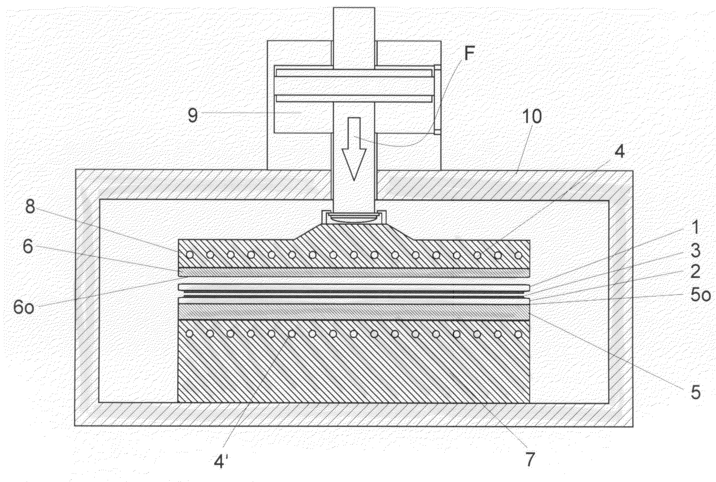
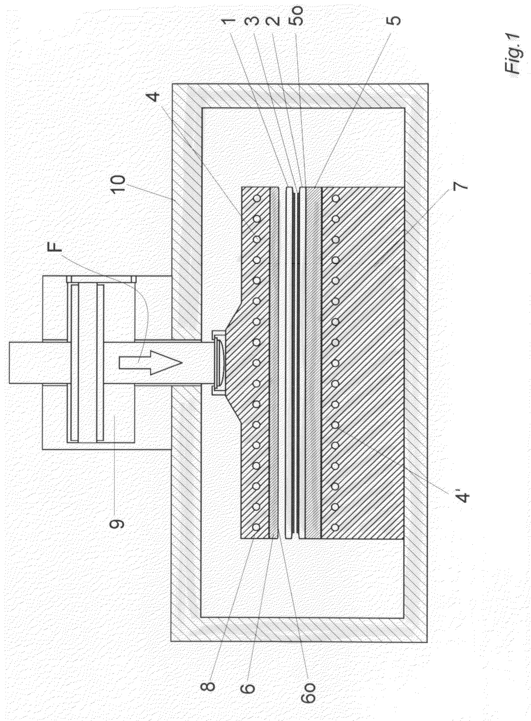
[0031]The single FIGURE shows a process chamber 10 with an opening, not shown, for loading and unloading substrates 1 and 2 and further connections, not shown, required for the process, on the upper side of which is located an actuator 9 for charging the substrates 1 and 2 with a pressing force F.

[0032]The pressing force F is transferred via an upper heating means 8 with heating coils 4 and an upper pressure plate 6 to the substrate lying on top.

[0033]The corresponding counter-force is transferred via the heating means 7 located on the base of the process chamber 10 and the lower pressure plate 5 lying on the heating means 7 to the substrate 2 held on the lower pressure plate 5. The substrates 1, 2 are bonded here by a (an optional) bonding layer 3. The lower heating means 7 has heating coils 4′ for heating the lower substrate 2.

[0034]If the upper pressure plate 6 is constructed from plastic, the substrates are heated in the process chamber 10 to a maximum temperature below 300° C.,...


PUM

PropertyMeasurementUnit
Temperatureaaaaaaaaaa

Abstract

The invention relates to a process and a device for bonding at least two substrates (1, 2), in particular semiconductor substrates or wafers, having the following features: a) a lower pressure plate (5) for holding the substrates (1, 2) and transferring pressure and, in particular, heat to the substrates (1, 2), b) an upper pressure plate (6) located opposite the lower pressure plate (5) for transferring pressure and, in particular, heat to the substrates (1, 2), c) heating means (7, 8) for heating up the substrates (1, 2), in particular to temperatures above 250° C., and d) pressure charging means, in particular an actuator (9), for charging the lower (5) and / or upper pressure plate (6) with a pressing force F, in particular higher than 500 N, preferably higher than 1,000 N. According to the invention, the upper pressure plate (6) and / or the lower pressure plate (5) are substantially free from the chemical elements Ti and Mo at least on one substrate contact surface (5o, 6o) facing the substrates.

Description

FIELD OF THE INVENTION[0001]The invention relates to a process and a device according to the preambles of claims 1 and 8.BACKGROUND OF THE INVENTION[0002]In the bonding of silicon wafers or semiconductor substrates (in the following: substrates), two substrates conventionally constructed as flat, circular discs—depending on the bonding process—are bonded to one another with a bonding layer, such as, for example, with adhesive (BCB, metal, solder) or without a bonding layer (SOI bonding or SDB bonding or anodic bonding) before further working steps.[0003]Because of the pressure required and the heating up and cooling down operations required, hard holding or pressure plates made of metal or alloyed with metal have hitherto been used to bond the substrates to one another.[0004]In this context, the substrates are loaded on to a lower holding plate in a process chamber. After the process chamber has been closed—depending on the bonding process—the process chamber is evacuated, if approp...

Claims


Application Information

Patent Timeline
IPC IPC(8): H01L21/30B29C65/02
CPCY10T156/10H01L21/67092H01L21/20H01L21/67132
Inventor THALLNER, ERICH
Owner THALLNER ERICH
Why Eureka
Try Eureka