Preparation method of film bulk acoustic wave resonator with isolation layer and bulk acoustic wave resonator

A bulk acoustic wave resonator, film bulk acoustic wave technology, applied in the direction of electrical components, impedance networks, etc., can solve the problems of film warping, fracture, and affecting the performance of cavity type bulk acoustic wave resonators, etc., to prevent damage to the sacrificial layer Effect

Active Publication Date: 2019-07-05
UNIV OF ELECTRONICS SCI & TECH OF CHINA
View PDF10 Cites 19 Cited by
  • Summary
  • Abstract
  • Description
  • Claims
  • Application Information

AI Technical Summary

Problems solved by technology

[0006] The object of the present invention is to provide a kind of thin-film bulk acoustic resonator preparation method and bulk acoustic wave resonator with isolation layer, through the design that isolation layer is set between lower electrode and bonding layer to solve existing bonding process, produce Bubbles in the single crystal film cause bubbles, causing the film to warp or sag or even break, which affects the technical problems of the performance of the cavity type bulk acoustic wave resonator

Method used


Image

  • Preparation method of film bulk acoustic wave resonator with isolation layer and bulk acoustic wave resonator
  • Preparation method of film bulk acoustic wave resonator with isolation layer and bulk acoustic wave resonator
  • Preparation method of film bulk acoustic wave resonator with isolation layer and bulk acoustic wave resonator

Examples


preparation example Construction

[0050] Such as figure 1 , figure 2 , image 3 , Figure 4 , Figure 5 , Figure 6 , Figure 7 , Figure 8 , Figure 9 and Figure 10 , a method for preparing a thin film bulk acoustic resonator with an isolation layer provided by the invention, comprising the steps of:

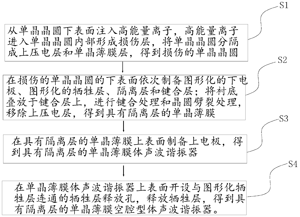
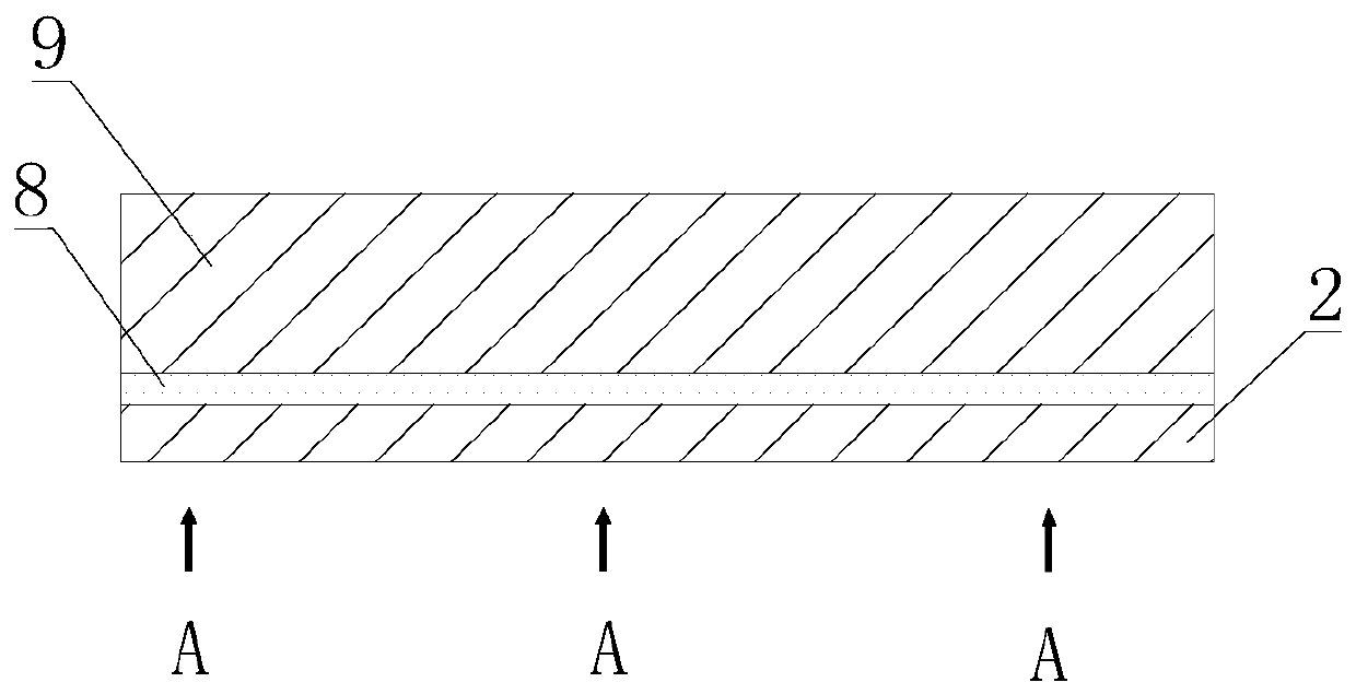
[0051] S1) High-energy ions A are injected from the lower surface of the single-crystal wafer, and the high-energy ions A enter the interior of the single-crystal wafer to form a damaged layer 8, and the single-crystal wafer is separated into an upper piezoelectric layer 9 and a single-crystal thin film layer 2, and the obtained Damaged single crystal wafers;

[0052] S2) Prepare a patterned lower electrode 3, a patterned sacrificial layer 10, an isolation layer 4, and a bonding layer 5 sequentially on the lower surface of the damaged single crystal wafer; stack the substrate 6 on the bonding layer, and perform Bonding treatment and wafer splitting treatment, removing the upper piezoelectric layer 9...

Embodiment 1

[0075] 1) A lithium niobate single crystal wafer is selected, and high-energy helium ions (He 2+ ), so that a damage layer is formed inside the lithium niobate single crystal wafer, and the damage layer separates the lithium niobate single crystal wafer into a lithium niobate upper piezoelectric layer and a lithium niobate single crystal film layer; He 2+ The implantation energy is 200keV, and the implantation depth is 0.6μm;

[0076] 2) The lower electrode is prepared on the lower surface of the lithium niobate single crystal thin film layer. The lower electrode can be prepared in two ways. The first method is to coat the lower surface of the lithium niobate single crystal thin film layer with photoresist (Ruihong AZ6212), forming a photoresist layer, using a patterned mask plate (made of chromium) to expose and develop the photoresist, growing a lower electrode, cleaning with acetone to remove the photoresist, and obtaining a patterned lower electrode; The two methods are t...

Embodiment 2

[0083] 1) A lithium niobate single crystal wafer is selected, and high-energy helium ions (He 2+ ), so that a damage layer is formed inside the lithium niobate single crystal wafer, and the damage layer separates the lithium niobate single crystal wafer into a lithium niobate upper piezoelectric layer and a lithium niobate single crystal film layer; He 2+The implantation energy is 200keV, and the implantation depth is 0.6μm;

[0084] 2) The lower electrode is prepared on the lower surface of the lithium niobate single crystal thin film layer. The lower electrode can be prepared in two ways. The first method is to coat the lower surface of the lithium niobate single crystal thin film layer with photoresist (Ruihong AZ6212), forming a photoresist layer, using a patterned mask plate (made of chromium) to expose and develop the photoresist, growing a lower electrode, cleaning with acetone to remove the photoresist, and obtaining a patterned lower electrode; The two methods are to...


PUM


Abstract

The invention relates to the technical field of acoustic wave resonator preparation, in particular to a preparation method of a film bulk acoustic wave resonator with an isolation layer and the bulk acoustic wave resonator. The method comprises the following steps: injecting high-energy ions from the lower surface of a single crystal wafer, enabling the high-energy ions to enter the single crystalwafer to form a damage layer, and dividing the single crystal wafer into an upper piezoelectric layer and a single crystal film layer to obtain a damaged single crystal wafer; sequentially preparinga graphical lower electrode, a graphical sacrificial layer, an isolation layer and a bonding layer on the lower surface of the single crystal film layer; stacking the substrate and the bonding layer,performing wafer splitting treatment, stripping the upper piezoelectric layer at the upper end of the single crystal film layer, and preparing an upper electrode on the upper surface of the single crystal film layer; and forming a sacrificial layer release hole required by the graphical sacrificial layer on the upper surface of the single crystal film layer, and releasing the sacrificial layer toobtain the high-quality cavity type bulk acoustic wave resonator of the single crystal film body.

Description

technical field [0001] The invention relates to the technical field of acoustic wave resonator preparation, in particular to a method for preparing a thin-film bulk acoustic wave resonator with an isolation layer and the bulk acoustic wave resonator. Background technique [0002] With the rapid development of wireless communication technology, traditional dielectric filters and surface acoustic wave filters are difficult to meet the high-frequency requirements. The new generation of thin film bulk acoustic resonators can meet this requirement well. The basic structure of thin film bulk acoustic resonators It is a simple three-layer structure, which is an upper electrode, a piezoelectric film and a metal isolation layer from top to bottom. The key to an acoustic resonator is the quality of the film. [0003] The current piezoelectric film mainly adopts the deposition method, which is difficult to ensure the lattice orientation of the film. In addition, the deposition on the ...

Claims


Application Information

Patent Timeline
Patent Type & Authority Applications(China)
IPC IPC(8): H03H3/02H03H9/02H03H9/17
CPCH03H3/02H03H9/02015H03H9/02086H03H9/171H03H2003/023
Inventor 吴传贵罗文博帅垚
Owner UNIV OF ELECTRONICS SCI & TECH OF CHINA
Why Eureka
Try Eureka