Optoelectronic systems providing high-power high-brightness laser light based on field coupled arrays, bars and stacks of semicondutor diode lasers

a laser light and semiconductor diode technology, applied in the direction of laser details, laser optical resonator construction, optical resonator shape and construction, etc., can solve the problems of limited output power, severe limitations of conventional prior art edge-emitting lasers, and limitations of optical power density of all technological improvements including facet passivation, zinc diffusion, or proton bombardmen

Active Publication Date: 2009-05-07
VI SYST GMBH
View PDF13 Cites 24 Cited by
  • Summary
  • Abstract
  • Description
  • Claims
  • Application Information

AI Technical Summary

Benefits of technology

[0015]In one embodiment of the present invention, a semiconductor optoelectronic device operating in a single lateral mode up to effective lateral output apertures is proposed. The device is based on an multilayer epitaxial structure operating as an effective broad vertical waveguide, which enables extension of the vertical near field up to a size exceeding three times the wavelength of light in the vacuum and beyond. In a preferred embodiment, the selection of a single vertical optical mode in a broad vertical waveguide is based on the phase matching effect. The vertical waveguide comprises two coupled cavities connected by a reflector. Light is generated in an active region placed in a first, thin cavity and partially leaks into a second, thick cavity, is reflected from the back side of the second cavity and returns to the active region, where it undergoes interference with light propagating in the first cavity. Phase matching conditions, and, hence, constructive interference are met for only one vertical mode which enables single vertical mode operation of the device. In one embodiment, the second thick cavity is just a substrate having preferably a mirror-like back side. In another embodiment, the second cavity is a thick epitaxially grown layer or a multilayer structure.
[0019]The leakage regions can be additionally formed on the sides from the lateral photonic band crystal. The lateral optical modes are discriminated in leakage loss and / or absorption loss. The single lateral mode light radiation can be obtained, upon a particular selection of a lateral photonic band crystal and a lateral optical defect, either in a fundamental optical mode providing a triple-lobe lateral far-field pattern, or in one of high-order lateral optical mode, providing a symmetric two-lobe far-field pattern, depending on the design. Special selection of a part of the lateral photonic band crystal close to its edge can enhance the discrimination of the lateral modes in leakage loss.
[0022]In one set of embodiments of the present invention, a system comprises an array of optoelectronic devices on a single wafer, wherein each of the devices emits a single lateral mode light having a low lateral beam divergence, and an array of external mirrors. The system operates in an edge-emitting geometry. Each optoelectronic device can be realized as a device having a lateral broad waveguide, a lateral flared waveguide, or a lateral photonic band crystal. In one embodiment of the present invention, each optoelectronic device operates as a gain chip. Each device comprises a lateral photonic band crystal. The gain chip emits light preferably in a single lateral mode, wherein emitted light has a three-lobe lateral far-field pattern. Light coming out in the side lobes from each pair of neighboring gain chips, impinges on a single mirror, thus providing optical coupling between light emitted by different gain chips. The array of gain chips and the array of external mirrors are selected such that the system emits laser light in a single lateral mode having a single-lobe far-field pattern with a narrow lateral beam divergence. Both a broad lateral waveguide and a thick vertical waveguide of each optoelectronic device in the system are preferred to ensure effective coupling of light emitted by each device and the formation of a single mode coherent laser light. This approach allows fabrication of an ultrabroad field coupled laser bar enabling ultrahigh power ultrahigh brightness lasing.
[0026]And yet another embodiment of the present invention includes a laser system comprising a stack of a few bars each of which is fabricated on a separated epitaxial wafer, and an array of external mirrors which couples both light emitted by optoelectronic devices on the same wafer and light emitted by optoelectronic devices on neighboring wafers. The devices and the external mirrors are selected such that the laser system provides coherent laser light in a single lateral optical mode extended throughout the entire stack. This approach allows fabrication of a field coupled laser stack enabling ultrahigh power ultrahigh brightness lasing.
[0028]Additionally, an electrooptical modulator element can be used in a laser of the present disclosure, wherein modulation of the refractive index in a part of the waveguide results in a frequency modulation of the emitted light, i.e. in modulation of the wavelength of the emitted laser light. This approach can provide an efficient speckle reduction.

Problems solved by technology

Conventional prior art edge emitting laser have severe limitations.
First, the output power is limited by the catastrophic optical mirror damage, and all technological improvements including facet passivation, zinc diffusion, or proton bombardment still have limitations in optical power density.
However, the lasing from broad area lasers is typically multimode and also suffers from beam filamentation which renders the laser radiation not focusable.
Using semiconductor diode laser as pump source for pumping solid state laser is extremely expensive.
Due to multi-mode lasing, the beam quality of the laser radiation from a broad area laser is low.
In addition, filamentation can occur which even more deteriorates the beam quality and renders the laser beam not focusable.
Such approach includes complex and expensive technological steps, i.e. etching and overgrowth and in fact does not prevent multi-mode lasing.
Conventional multistripe processing, which is cost-effective, does not enable single mode operation either.
This hinders the formation of a single coherent optical field and thus leads to filamentation of the emitted laser light, and no benefit in brightness or focuseability may be expected.

Method used


Image

  • Optoelectronic systems providing high-power high-brightness laser light based on field coupled arrays, bars and stacks of semicondutor diode lasers
  • Optoelectronic systems providing high-power high-brightness laser light based on field coupled arrays, bars and stacks of semicondutor diode lasers
  • Optoelectronic systems providing high-power high-brightness laser light based on field coupled arrays, bars and stacks of semicondutor diode lasers

Examples


Embodiment Construction

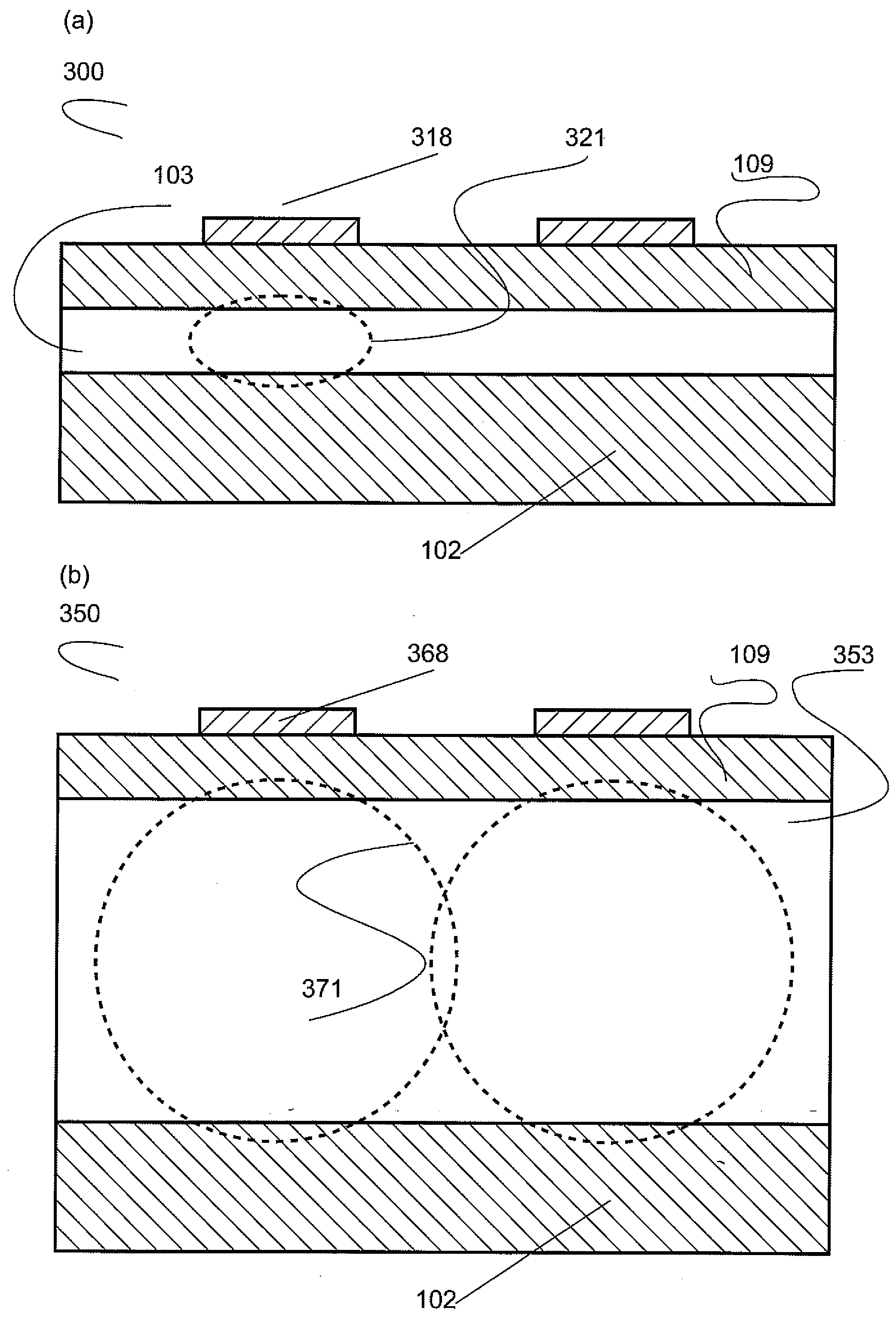
[0089]FIG. 3(b) shows a different situation as compared to FIG. 3(a). The laser (350) contains a waveguide (353) which is broad in the vertical direction. This means that the waveguide is preferably broader than three times the wavelength of the generated laser light in the vacuum. Let, for example, the waveguide have a width of 10 micrometers. This can be comparable with the lateral distance between the centers of neighboring ridges (368). In this case, the profile of the optical field generated underneath each ridge has a shape close to the round shape (371), and optical fields generated underneath neighboring ridges, can overlap. Then, a coherent lateral optical field can be created across the laser.

[0090]A serious obstacle which typically hinders using a broad vertical waveguide is connected with the fact that the lasing from a broad waveguide is usually multi-mode. Special new concepts have to be implemented in order to ensure a single vertical mode lasing from a broad vertical...


PUM


Abstract

A semiconductor diode laser having a broad vertical waveguide and a broad lateral waveguide is disclosed emitting laser-light in a single vertical mode and a single lateral mode narrow beam. The vertical waveguide comprises a coupled cavity structure, wherein light, generated in the active medium placed in the first cavity leaks into the second cavity and returns back. Phase matching conditions govern the selection of a single vertical mode. A multi-stripe lateral waveguide comprises preferably a lateral photonic band crystal with a lateral optical defect created by selected pumping of multistripes. This approach allows the selection of a single lateral mode having a higher optical confinement factor and / or a lower absorption loss and / or a lower leakage loss compared to the rest lateral optical modes. This enables a single lateral mode lasing from a broad area field coupled laser array. A laser system comprised of multiple field coupled laser arrays on a single wafer and a set of external mirrors enables an ultra-broad field coupled laser bar emitting a coherent laser light in a single vertical optical mode and a single lateral optical mode. A laser system comprised of multiple ultra-broad field coupled laser bars on different wafers and a set of external mirrors enables an ultra-broad field coupled laser stack emitting coherent laser light in a single vertical optical mode and a single lateral optical mode. This allows realization of ultrahigh power ultrahigh brightness laser systems based on semiconductor diode lasers.

Description

REFERENCE TO RELATED APPLICATIONS[0001]This is a continuation-in-part of U.S. patent application Ser. No. 11 / 453,980, filed Jun. 16, 2006, entitled “EXTERNAL CAVITY OPTOELECTRONIC DEVICE”, U.S. patent application Ser. No. 11 / 648,551, filed Jan. 3, 2007, entitled “OPTOELECTRONIC DEVICE AND METHOD OF MAKING SAME”, and PCT Patent Application PCT / IB2007 / 1004283, filed Jun. 6, 2007, entitled “OPTOELECTRONIC DEVICE AND METHOD OF MAKING SAME”. The aforementioned applications are hereby incorporated herein by reference.BACKGROUND OF THE INVENTION[0002]1. Field of the Invention[0003]The invention pertains to the field of semiconductor optoelectronic devices. More particularly, the invention pertains to high-power high-brightness semiconductor diode lasers with a narrow beam divergence and to arrays, bars and stacks based thereupon.[0004]2. Description of Related Art[0005]There is a need in high-power semiconductor diode lasers for numerous application including, but not limited to welding, m...

Claims


Application Information

Patent Timeline
Patent Type & Authority Applications(United States)
IPC IPC(8): H01S5/026
CPCH01S5/0265H01S5/028H01S5/0604H01S5/0605H01S5/10H01S5/1021H01S2301/18H01S5/105H01S5/14H01S5/2036H01S5/32341H01S5/4031H01S5/4081H01S5/1032H01S5/11
Inventor SHCHUKIN, VITALYLEDENTSOV, NIKOLAI
Owner VI SYST GMBH
Why Eureka
Try Eureka