

Wafer three-dimensional integrated lead wire process for three-dimensional memory and structure thereof
A technology of integrated leads and three-dimensional storage, which is applied in the manufacture of electric solid-state devices, semiconductor devices, semiconductor/solid-state devices, etc., can solve problems such as difficulties in leading out the first metal layer, achieve the effects of reducing production costs and improving product yields
- Summary
- Abstract
- Description
- Claims
- Application Information
AI Technical Summary
Problems solved by technology
Method used
Image

Examples
Embodiment 1
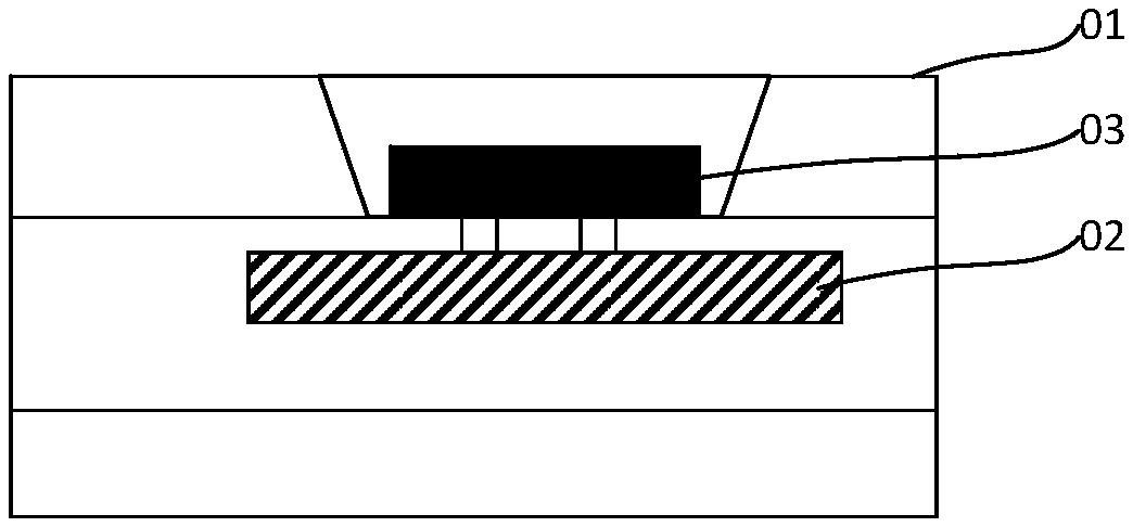
[0041] refer to Figure 3-8 As shown, Embodiment 1 of the present invention provides a wafer three-dimensional integrated wiring process, including the following steps:
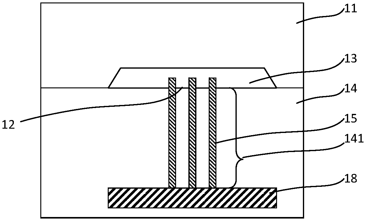
[0042] A first wafer 11 is provided, the first wafer 11 has a front side and a back side arranged oppositely, and a contact hole area 12 is provided on at least a part of the front side of the first wafer 11;
[0043] A dielectric layer 13 is formed in the contact hole region 12, the dielectric layer 13 is an oxide dielectric layer 13 or a nitride dielectric layer 13, and the process of forming the dielectric layer 13 in the contact hole region 12 includes lithography, etching, deposition , one of filling and grinding or any combination thereof, the dielectric layer has a top surface and a bottom surface oppositely arranged, wherein the top surface is the side facing the front side of the first wafer, and the bottom surface is the side facing the back side of the first wafer side;
[0044] A semiconductor dev...
Embodiment 2
[0053] In this embodiment, the parts different from the above embodiments will be described, and the same parts will not be repeated.
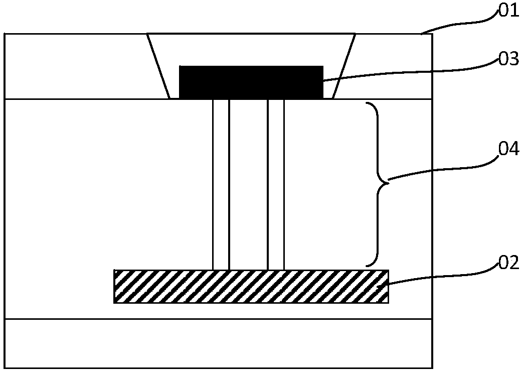
[0054] refer to image 3 As shown, the dielectric layer 13 has a bottom surface and a top surface oppositely disposed, and the bottom surface is a side farther away from the first metal layer 18 than the top surface. In the step of forming the dielectric layer 13, at first, a shallow trench is formed in the contact hole region 12 on the front surface of the first wafer 11 by lithography and etching processes, and then a shallow trench is formed in the shallow trench by deposition and filling processes. The dielectric layer 13 is formed in the groove, and the dielectric layer 13 may be ground to be planarized by a grinding process later. After the above process steps, the bottom surface of the formed dielectric layer 13 is located inside the first wafer 11 , and the top surface of the dielectric layer 13 is flush with the front surface of the ...
Embodiment 3
[0064] In this embodiment, the parts different from the above embodiments will be described, and the same parts will not be repeated.
[0065] The dielectric layer 13 has a bottom surface and a top surface opposite to each other, and the bottom surface is a side farther away from the first metal layer 18 than the top surface. In the step of forming the dielectric layer 13, at first, a shallow trench is formed in the contact hole region 12 on the front surface of the first wafer 11 by lithography and etching processes, and then a shallow trench is formed in the shallow trench by deposition and filling processes. The dielectric layer 13 is formed in the groove, and the dielectric layer 13 may be ground to be planarized by a grinding process later. After the above process steps, the bottom surface of the formed dielectric layer 13 is located inside the first wafer 11 , and the top surface of the dielectric layer 13 is higher than the front surface of the first wafer 11 .
PUM
| Property | Measurement | Unit |
|---|---|---|
| Thickness | aaaaa | aaaaa |
Abstract
Description
Claims
Application Information