Photoresist structure, graphical deposition layer, semiconductor chip, and manufacturing methodd of photoresist structure, graphical deposition layer and semiconductor chip

A technology for a photoresist layer and a fabrication method, applied in the field of patterned deposition layers, semiconductor chips and their fabrication, and photoresist structures, can solve the problem of reducing process compatibility, adhesion, and discrepancies between the actual size of the patterned deposition layer and the defined size and other problems, to achieve the effect of reducing peeling difficulty and peeling cost

A technology for a photoresist layer and a fabrication method, applied in the field of patterned deposition layers, semiconductor chips and their fabrication, and photoresist structures, can solve the problem of reducing process compatibility, adhesion, and discrepancies between the actual size of the patterned deposition layer and the defined size and other problems, to achieve the effect of reducing peeling difficulty and peeling cost

CN112652522AActive Publication Date: 2021-04-13TENCENT TECH (SHENZHEN) CO LTD

Image

  • Photoresist structure, graphical deposition layer, semiconductor chip, and manufacturing methodd of photoresist structure, graphical deposition layer and semiconductor chip
  • Photoresist structure, graphical deposition layer, semiconductor chip, and manufacturing methodd of photoresist structure, graphical deposition layer and semiconductor chip
  • Photoresist structure, graphical deposition layer, semiconductor chip, and manufacturing methodd of photoresist structure, graphical deposition layer and semiconductor chip

Examples


Embodiment Construction

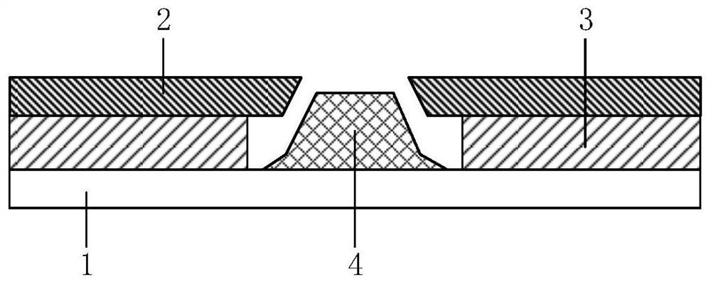
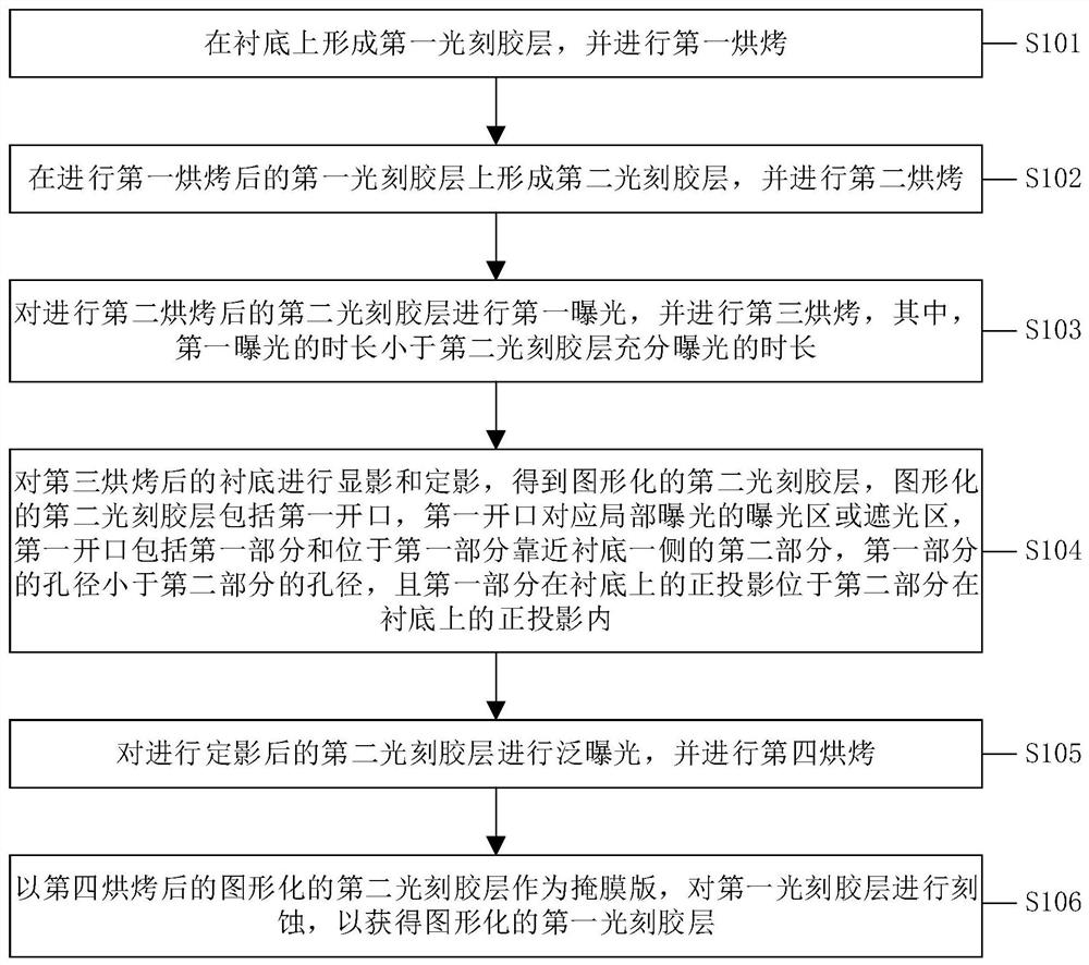
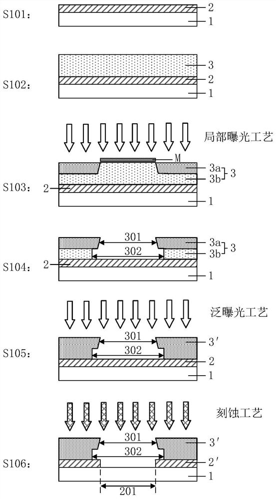
[0041] The present application is described in detail below, and examples of embodiments of the present application are shown in the drawings, wherein the same or similar reference numerals denote the same or similar components or components having the same or similar functions throughout. Also, detailed descriptions of known technologies will be omitted if they are not necessary to illustrate the features of the present application. The embodiments described below by referring to the figures are exemplary only for explaining the present application, and are not construed as limiting the present application.

[0042] Those skilled in the art can understand that, unless otherwise defined, all terms (including technical terms and scientific terms) used herein have the same meanings as commonly understood by those of ordinary skill in the art to which this application belongs. It should also be understood that terms, such as those defined in commonly used dictionaries, should be ...


PUM


Abstract

The embodiment of the invention provides a photoresist structure, a graphical deposition layer, a semiconductor chip, and manufacturing methods of the photoresist structure, the graphical deposition layer and the semiconductor chip. According to the manufacturing method of the photoresist structure, a single photoresist is utilized, the second photoresist layer containing the undercut can be obtained only by using a single developing solution for one-time development, and the size of the undercut can be controlled through the development time, so the problems of stripping difficulty and the like caused by adhesion of a deposition material and the side wall of the photoresist structure in a traditional stripping process are avoided; the first photoresist layer is used as a protective adhesive layer, so that corrosion damage of a developing solution to a substrate material during development can be avoided; and the first photoresist layer is etched, so that the first photoresist layer serving as a protective adhesive layer is converted into a pattern limiting adhesive layer, lateral diffusion at the bottom of a deposition material can be effectively prevented in the material deposition process, and the deposition layer with good morphology is obtained.

Description

technical field [0001] The invention relates to the technical field of micro-nano processing, in particular to a photoresist structure, a patterned deposition layer, a semiconductor chip and a manufacturing method thereof. Background technique [0002] In the field of micro-nano processing technology, most of the processing technology, such as lift-off technology, needs to be realized by preparing a special photoresist structure. [0003] Taking the lift-off process as an example, the following problems have always existed in the traditional technology: first, the sidewall of the deposition material is easy to adhere to the sidewall of the photoresist, resulting in poor morphology of the patterned deposition layer; second, the photoresist pattern During the chemicalization process, the developer will react with the substrate material and cause corrosion to the substrate material. [0004] For the first problem, it can usually be solved by preparing a photoresist structure c...

Claims


Application Information

Patent Timeline
13 Apr 2021
Publication
CN112652522A
IPC
H01L21/027; H01L21/32; H01L21/3205
CPC
H01L21/0271; H01L21/32; H01L21/3205; G03F7/095; G03F7/168; G03F7/38; G03F7/2014; G03F7/40
Inventors
张文龙; 郑亚锐