Photostimulation two-end artificial synaptic device and preparation method and application thereof
A technology of synaptic devices and light stimulation, which is applied in the direction of electrical components, etc., can solve the problems of speed limitation of simulated synaptic devices, and achieve the effects of easy implementation, low energy consumption and low cost
- Summary
- Abstract
- Description
- Claims
- Application Information
AI Technical Summary
Problems solved by technology
Method used
Image

Examples
Embodiment 1
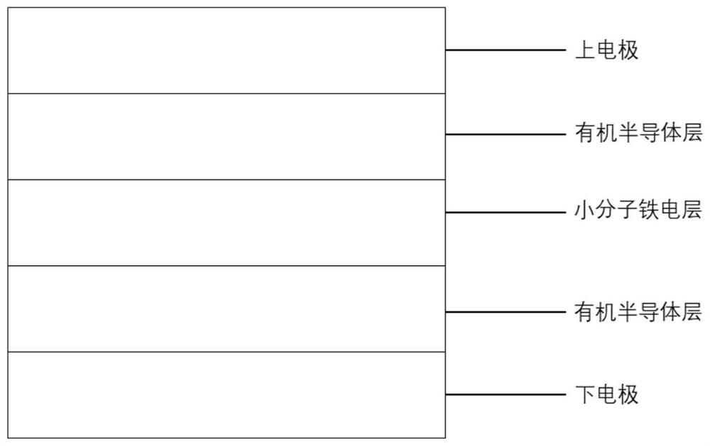
[0042] In this embodiment, guanidinium perchlorate C (NH 2 ) 3 ClO 4 It is a small molecule ferroelectric layer, and phthalocyanine (CuPc) is used as an organic semiconductor layer, which have the following structures:
[0043]
[0044] Preparation of artificial synaptic devices based on conductive polymers, the specific steps are as follows:
[0045] (1) Clean the lower electrode, put the lower electrode in deionized water for 1 to 3 minutes, then put it in acetone solution for 1 to 3 minutes, then put it in isopropanol for 1 to 3 minutes, and finally Put the lower electrode into a vacuum oven to dry;
[0046](2) To prepare small molecule ferroelectrics, react guanidinium perchlorate with guanidine carbonate and perchloric acid in a ratio of 1:1 in an aqueous solution to synthesize guanidinium perchlorate, let it evaporate slowly, and obtain colorless and transparent after 48 hours of crystals. Wherein, the concentration of perchloric acid is 0.05~1mol / L, the concentr...
Embodiment 2
[0053] The present embodiment uses tetraethyl ammonium perchlorate (C 8 h 20 ClNO 4 ) is a small molecule ferroelectric layer, and copper phthalocyanine (CuPc) is used as an organic semiconductor layer, which has the following structure respectively:
[0054]
[0055] Preparation of artificial synaptic devices based on conductive polymers, the specific steps are as follows:
[0056] (1) Clean the lower electrode, put the lower electrode in deionized water for 1 to 3 minutes, then put it in acetone solution for 1 to 3 minutes, then put it in isopropanol for 1 to 3 minutes, and finally Put the lower electrode into a vacuum oven to dry;
[0057] (2), vacuum evaporation organic semiconductor layer, on the lower electrode that step (1) obtains, thermal evaporation deposits a layer of phthalocyanine copper organic semiconductor layer, puts phthalocyanine copper material in the quartz crucible in the vacuum thermal evaporator , when the vacuum degree of the vacuum evaporation ...
PUM
| Property | Measurement | Unit |
|---|---|---|
| thickness | aaaaa | aaaaa |
| thickness | aaaaa | aaaaa |
| thickness | aaaaa | aaaaa |
Abstract
Description
Claims
Application Information
 - R&D Engineer
- R&D Manager
- IP Professional
- Industry Leading Data Capabilities
- Powerful AI technology
- Patent DNA Extraction
Browse by: Latest US Patents, China's latest patents, Technical Efficacy Thesaurus, Application Domain, Technology Topic.
© 2024 PatSnap. All rights reserved.Legal|Privacy policy|Modern Slavery Act Transparency Statement|Sitemap