Optoelectronic device, circuit module and switch with lamp

A technology of optoelectronic devices and circuit modules, applied in the direction of electric switches, printed circuits connected with non-printed electrical components, circuits, etc., can solve the problems of damaged LED lamp beads, insufficient reliability, low yield rate, etc., and achieve reduction Effects of damage, increased reliability, and reduced chance of damage

Pending Publication Date: 2021-04-30
郑华军
View PDF0 Cites 0 Cited by
  • Summary
  • Abstract
  • Description
  • Claims
  • Application Information

AI Technical Summary

Problems solved by technology

[0003] Optoelectronic devices with pins, which can easily damage the optoelectronic chip when the pins are bent
For example, when LED lamp beads are soldered and installed, the pins of LED lamp beads generally need to be bent to facilitate fixing. The force of the foot is transmitted to the LED lamp bead, which easily damages the inside of the LED lamp bead, resulting in a low yield rate and insufficient reliability

Method used


Image

  • Optoelectronic device, circuit module and switch with lamp
  • Optoelectronic device, circuit module and switch with lamp
  • Optoelectronic device, circuit module and switch with lamp

Examples


Embodiment Construction

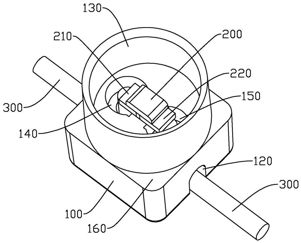
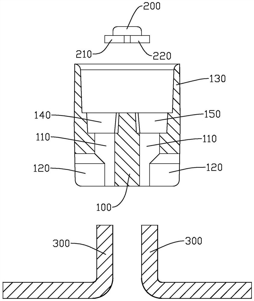
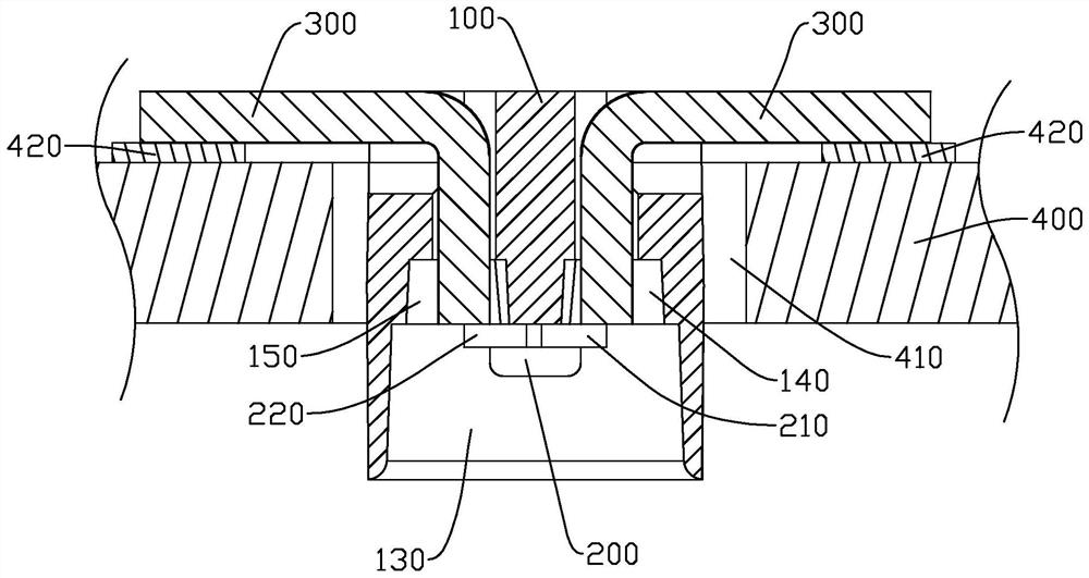
[0028] Embodiments of the present invention are described in detail below, examples of which are shown in the drawings, wherein the same or similar reference numerals designate the same or similar elements or elements having the same or similar functions throughout. The embodiments described below by referring to the figures are exemplary only for explaining the present invention and should not be construed as limiting the present invention.

[0029] In the description of the present invention, it should be understood that the orientation descriptions, such as up, down, front, back, left, right, etc. indicated orientations or positional relationships are based on the orientations or positional relationships shown in the drawings, and are only In order to facilitate the description of the present invention and simplify the description, it does not indicate or imply that the device or element referred to must have a specific orientation, be constructed and operated in a specific ...


PUM


Abstract

The invention discloses an optoelectronic device, a circuit module and a switch with a lamp. The optoelectronic device comprise a base; a photoelectronic chip which is arranged on the base; and a conductive pin, wherein the base is provided with a guide channel, the conductive pin is arranged in the guide channel in a penetrating manner, and the conductive pin is connected with the photoelectronic chip. The base is provided with the guide channel, the conductive pin penetrates through the guide channel to be connected with the photoelectronic chip, and the part, located in the guide channel, of the conductive pin is limited by the guide channel and can only move along the length direction of the guide channel, so that when the conductive pin is bent by external force, the acting force mainly acts on the wall surface, forming the guide channel, of the base, and the influence of the acting force on the photoelectronic chip is very small. Therefore, when the conductive pins are stressed and bent, the effect of reducing damage to the photoelectronic chip is achieved, and the reliability is improved.

Description

technical field [0001] The invention relates to the field of optoelectronic devices, in particular to an optoelectronic device, a circuit module and a switch with lights. Background technique [0002] With the development of optoelectronic technology, optoelectronic devices such as LED chips and photosensitive chips are widely used in different fields to meet various usage needs. Among them, LED chips, as a new generation of lighting devices, have the advantages of energy saving, high light efficiency, and long service life. In order to meet different usage requirements, LEDs come in various sizes, packages, and welding methods. [0003] For optoelectronic devices with pins, it is easy to damage the optoelectronic chip when the pins are bent. For example, when LED lamp beads are soldered and installed, the pins of LED lamp beads generally need to be bent to facilitate fixing. The force of the foot is transmitted to the LED lamp bead, which easily damages the inside of the...

Claims


Application Information

Patent Timeline
Patent Type & Authority Applications(China)
IPC IPC(8): H01L33/48H01L33/62H05K1/18H01H9/02
CPCH01H9/0271H01L33/48H01L33/62H05K1/184
Inventor 郑华军
Owner 郑华军
Why Eureka
Try Eureka