Circuit board and its non-inductive scratch repair process

A circuit board and process technology, applied in the field of circuit board and its non-inductive scratch repair process, can solve problems such as the elimination of difficult appearance, circuit board scratches, and complicated circuit board preparation process, so as to improve the repair effect and improve the appearance Effect

Active Publication Date: 2022-01-18
CAMELOT QINGYUAN HYTEC TECH INVESTMENT
View PDF4 Cites 0 Cited by
  • Summary
  • Abstract
  • Description
  • Claims
  • Application Information

AI Technical Summary

Problems solved by technology

[0002] The preparation process of circuit boards is complicated, and may need to be transferred to multiple assembly lines for processing during the preparation process. During each transfer and processing process, there may be problems with scratches on circuit boards, and it is difficult to distinguish and more common. The surface of the solder resist layer is scratched, and there are two types of scratches. One is felt scratches. Obvious scratches can be seen on the surface of the solder mask and the existence of scratches can be clearly felt after contact. The scratches formed by scratches will seriously affect the quality of the circuit board; the other is non-inductive scratches, where obvious scratches can be seen on the surface of the solder mask but cannot be clearly felt after contact. This kind of scratch basically exists in each circuit board, and the scratches formed by non-inductive scratches will affect the appearance of the circuit board. The scratches required to be repaired, but it is difficult to eliminate the scratches formed by non-inductive scratches in the existing technology

Method used


Image

  • Circuit board and its non-inductive scratch repair process

Examples


Embodiment 1

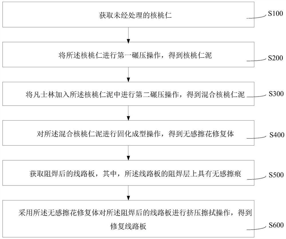
[0059] Peel the untreated walnut kernels, put 800g of the peeled walnut kernels into a mortar and grind them until they can be scattered by hand, then add 200g of Vaseline and 21g of paraffin into the mortar Carry out further rolling, pass the mixed walnut kernel mud obtained by rolling through a 400-mesh sieve, squeeze and solidify the sieved mixed walnut kernels into a block-shaped non-sensitivity scratch restoration, and restore the block-like non-sensitivity scratch Wipe the solder resist layer on the circuit board at a wiping speed of 200mm / s.

Embodiment 2

[0061] Peel the untreated walnut kernels, put 850g of the peeled walnut kernels into a mortar and grind them until they can be scattered by hand, then add 140g of Vaseline and 49g of paraffin into the mortar Carry out further rolling, pass the mixed walnut kernel mud obtained by rolling through a 400-mesh sieve, squeeze and solidify the sieved mixed walnut kernels into a block-shaped non-sensitivity scratch restoration, and restore the block-like non-sensitivity scratch Wipe the solder resist layer on the circuit board at a wiping speed of 250mm / s.

Embodiment 3

[0063] Peel the untreated walnut kernels, put 900g of the peeled walnut kernels into a mortar and grind them until they can be scattered by hand, then add 180g of Vaseline and 81g of paraffin into the mortar Carry out further rolling, pass the mixed walnut kernel mud obtained by rolling through a 500-mesh sieve, squeeze and solidify the sieved mixed walnut kernels into a block-like non-sensitivity scratch restoration, and restore the block-like non-sensitivity scratch Wipe the solder mask on the circuit board at a wiping speed of 300mm / s.


PUM


Abstract

The present application provides a non-inductive scratch repair process for circuit boards. The above-mentioned non-inductive rubbing repair process for circuit boards includes the following steps: obtaining untreated walnut kernels; performing a first rolling operation on the walnut kernels to obtain walnut kernel mud; adding Vaseline to the walnut kernel mud for a second rolling operation , to obtain mixed walnut kernel paste; solidify and form the mixed walnut kernel paste to obtain a non-inductive scratch restoration; obtain a circuit board after solder masking, wherein there are non-inductive scratches on the solder mask layer of the circuit board; Squeeze and wipe the circuit board after the solder resistance with the scratch-scratch restoration body to obtain the repaired circuit board. The above-mentioned non-inductive scratch repair process for circuit boards can better repair the non-inductive scratches and improve the appearance of the circuit board.

Description

technical field [0001] The invention relates to the technical field of circuit boards, in particular to a circuit board and its non-inductive scratch repair process. Background technique [0002] The preparation process of circuit boards is complicated, and may need to be transferred to multiple assembly lines for processing during the preparation process. During each transfer and processing process, there may be problems with scratches on circuit boards, and it is difficult to distinguish and more common. The surface of the solder resist layer is scratched, and there are two types of scratches. One is felt scratches. Obvious scratches can be seen on the surface of the solder mask and the existence of scratches can be clearly felt after contact. The scratches formed by scratches will seriously affect the quality of the circuit board; the other is non-inductive scratches, where obvious scratches can be seen on the surface of the solder mask but cannot be clearly felt after co...

Claims


Application Information

Patent Timeline
Patent Type & Authority Patents(China)
IPC IPC(8): H05K3/00
CPCH05K3/00H05K2203/17H05K2203/12
Inventor 赖泳芝郭亮亮彭甜甜
Owner CAMELOT QINGYUAN HYTEC TECH INVESTMENT
Why Eureka
Try Eureka