
A terahertz detector with integrated silicon photonic crystal waveguide

A terahertz detector and photonic crystal waveguide technology, applied in the field of terahertz detection, can solve the problems of loss of coupling resonance and filtering, reduce detector coupling energy, reduce detector sensitivity, etc., and achieve small transmission loss and preparation process compatibility Good, the effect of improving the coupling efficiency

Active Publication Date: 2022-03-25
NANJING UNIV
View PDF8 Cites 0 Cited by
  • Summary
  • Abstract
  • Description
  • Claims
  • Application Information

AI Technical Summary

Problems solved by technology

Due to the characteristics of the photonic crystal itself, its design generally only has a single-frequency filter module, which cannot realize coupling filtering in multiple frequency bands; multiple coupling filter modules are combined on the same photonic crystal plate by splicing and usually lose their originality due to lattice mismatch. The function of coupling resonance and filtering of each frequency band
Especially in the terahertz band, the wavelength of the incident terahertz signal is usually above 100 microns, and the size of the photonic crystal waveguide is much larger than that in the optical band, and the terahertz wave has a large attenuation during propagation, which greatly reduces the detection The energy coupled by the detector reduces the sensitivity of the detector

Method used


Image

  • A terahertz detector with integrated silicon photonic crystal waveguide
  • A terahertz detector with integrated silicon photonic crystal waveguide
  • A terahertz detector with integrated silicon photonic crystal waveguide

Examples


Embodiment

[0036] In order to verify the effectiveness of the scheme of the present invention, the following simulation calculations are performed.

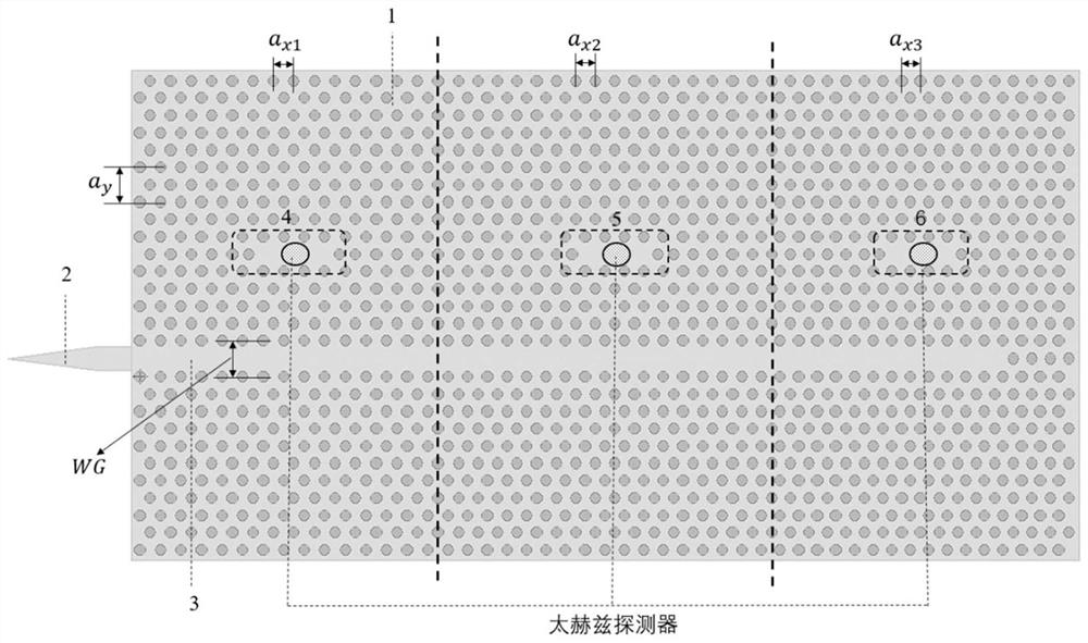
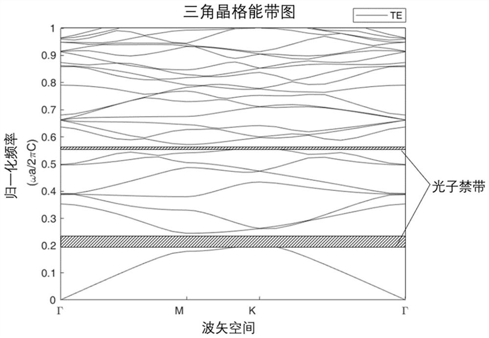
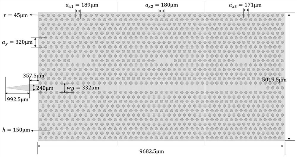
[0037] This embodiment provides a terahertz detector integrated with a silicon photonic crystal waveguide, such as figure 1As shown, it includes a two-dimensional photonic crystal slab 1, a graded coupling input waveguide 2, a line defect transmission waveguide 3, three L3 photonic microcavities 4, 5, 6, and three terahertz lasers integrated in the center of the L3 photonic microcavity. detector. In order to determine the structural parameters of the two-dimensional silicon photonic crystal waveguide, the bandgap theory of photonic crystal is used to design. The steps of the design method and the analysis of the results are as follows:

[0038] 1) Calculate the energy band structure of photonic crystals

[0039] Starting from Maxwell's equations, the intrinsic equations of electromagnetic waves in photonic crystals are deduced by using th...


PUM

PropertyMeasurementUnit
thicknessaaaaaaaaaa

Abstract

The present invention proposes a terahertz detector integrating a silicon photonic crystal waveguide, including a two-dimensional photonic crystal plate, a gradient coupling input waveguide, a line defect transmission waveguide, multiple L3-type photonic microcavities, and multiple terahertz detectors. Among them: the two-dimensional photonic crystal plate is composed of several crystal units, and the lattice on each crystal unit is arranged periodically to form a triangular lattice structure. The horizontal lattice constants on different crystal units are different, while the vertical lattice constants are the same, so as to maintain the crystal The horizontal splicing of the unit block corresponds; each crystal unit is equipped with an L3 photonic microcavity, and each L3 photonic microcavity is equipped with a terahertz detector. Each crystal unit is connected by a line defect transmission waveguide, and the two-dimensional photonic crystal The plate is connected with the external input waveguide through the gradient coupling input waveguide. The invention can simultaneously detect terahertz signals in multiple frequency bands.

Description

technical field [0001] The invention relates to terahertz detection technology, in particular to a terahertz detector integrated with a silicon photonic crystal waveguide. Background technique [0002] Terahertz spectrum usually refers to the spectrum region between 0.1THz and 10THz, corresponding to a wavelength of 30-3000μm. Its special spectral position determines its irreplaceable application in biological imaging and high-speed wireless communication. As an indispensable device in the field of terahertz detection, terahertz detectors are still an urgent problem to be solved in the field of terahertz how to make detectors with simple structure and easy integration. Compared with electrons in the medium, terahertz light waves are difficult to confine and store, and the speed is difficult to control. Photonic crystals are expected to solve this problem, allowing people to manipulate light waves in a medium. Photonic crystals are a new type of functional material whose di...

Claims


Application Information

Patent Timeline
Patent Type & Authority Patents(China)
IPC IPC(8): G01J1/42G02B6/122G02B6/293
CPCG01J1/42G02B6/29335G02B6/1225
Inventor 涂学凑张祎琛周淑宇蒋成涛贾小氢赵清源张蜡宝康琳陈健吴培亨
Owner NANJING UNIV
Learn More