Chip welding device for PCB and circuit board preparation process

A technology for chip welding and board use, which is applied in the field of chip welding devices for PCB circuit boards and circuit board preparation technology, and can solve the problems of time-consuming and laborious operations, inconvenient operations, and difficult handling of white smoke.

Inactive Publication Date: 2021-05-07
合肥坤雄智能制造有限公司
View PDF0 Cites 2 Cited by
  • Summary
  • Abstract
  • Description
  • Claims
  • Application Information

AI Technical Summary

Problems solved by technology

[0005] Aiming at the deficiencies of the prior art, the present invention provides a chip welding device for PCB circuit boards, which has the advantages of being easy to flip, adjusting the angle position, and being able to deal with white smoke generated by welding, etc. Smoke is not easy to deal with

Method used


Image

  • Chip welding device for PCB and circuit board preparation process
  • Chip welding device for PCB and circuit board preparation process
  • Chip welding device for PCB and circuit board preparation process

Examples


Embodiment Construction

[0034] The following will clearly and completely describe the technical solutions in the embodiments of the present invention with reference to the accompanying drawings in the embodiments of the present invention. Obviously, the described embodiments are only some, not all, embodiments of the present invention. Based on the embodiments of the present invention, all other embodiments obtained by persons of ordinary skill in the art without making creative efforts belong to the protection scope of the present invention.

[0035]As described in the background technology, there are deficiencies in the prior art. In order to solve the above technical problems, the application proposes a chip welding device for PCB circuit boards.

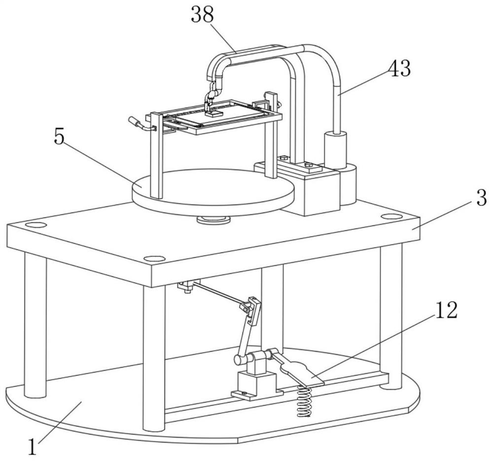
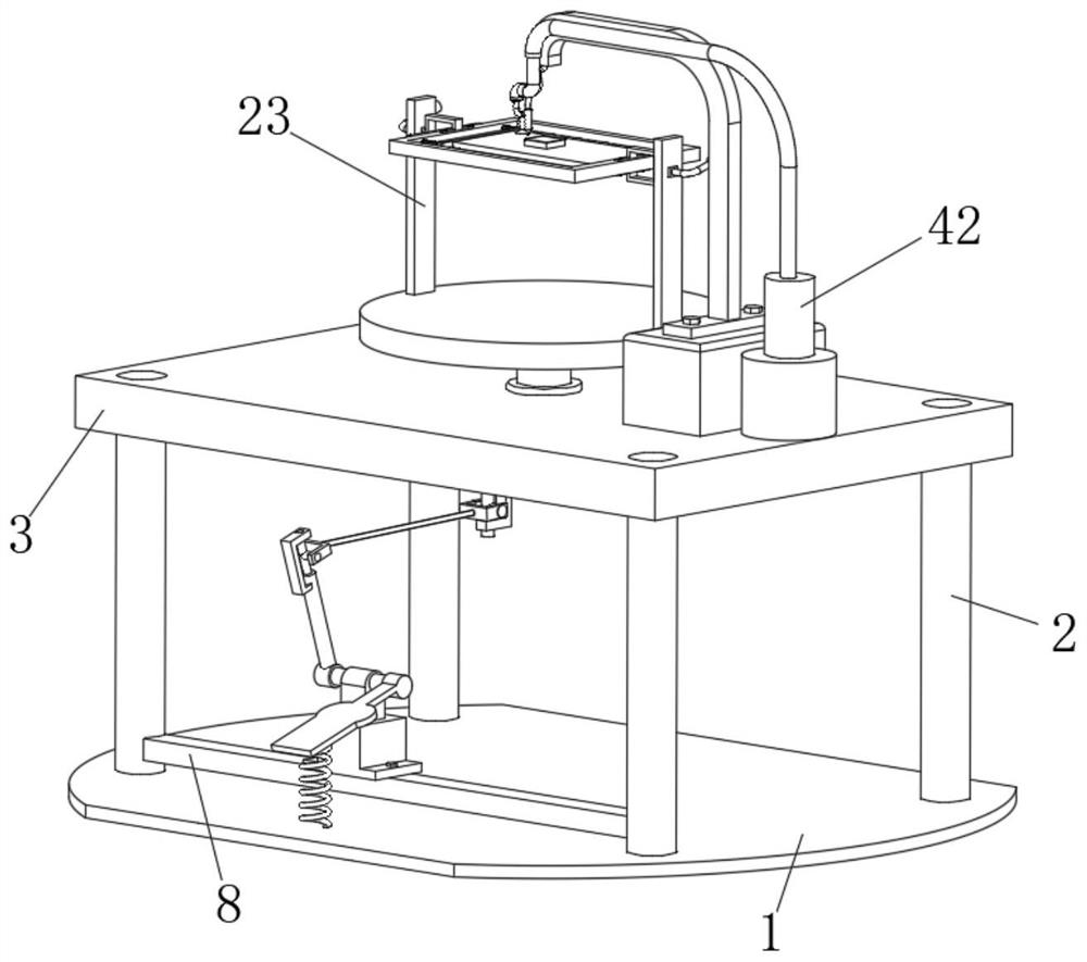
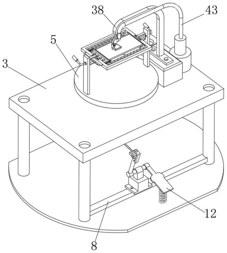
[0036] In a typical implementation of the present application, such as Figure 1-10 As shown, a chip welding device for a PCB circuit board includes a bottom plate 1, four pillars 2 are fixedly connected to the top of the bottom plate 1 when it is heate...


PUM


Abstract

The invention relates to the technical field of chip welding devices, and discloses a chip welding device for a PCB and a circuit board preparation process. A pedal plate is pressed downwards to enable a rotating shaft to rotate, the rotating shaft drives a first connecting rod to swing, then a linkage rod is driven by a second U-shaped frame, a fourth U-shaped frame and a second cross-shaped block are driven to swing through the linkage rod, then a rotating block is driven, a fixing sleeve is driven through the rotating block to enable the rotating shaft to rotate, a rotating disc is enabled to rotate through the rotating shaft, the fixing frame is driven to rotate along with the rotating shaft, different welding positions of a circuit board and a chip body can be adjusted, two rotating handles are rotated to drive two U-shaped handles to rotate, the fixing frame is enabled to rotate through the two U-shaped handles, then the circuit board and the chip body are enabled to rotate, and the two rotating handles are loosened after the circuit board and the chip body are rotated to a proper angle, so that the other surface of the circuit board can be welded through the rectangular hole, operation inconvenience caused by manual overturning is prevented, and then the welding speed is increased.

Description

technical field [0001] The invention relates to the technical field of chip welding devices, in particular to a chip welding device for a PCB circuit board and a circuit board preparation process. Background technique [0002] Circuit boards, circuit boards, PCB boards, and soldering technology have developed in the electronics industry in recent years. It can be noticed that an obvious trend is reflow soldering technology. In principle, traditional inserts can also be used for reflow soldering. The advantage of through-hole reflow soldering is that it is possible to complete all solder joints at the same time, which minimizes production costs. However, temperature-sensitive components limit the application of reflow soldering, whether it is a plug-in or SMD, and then people put Turning to selective soldering, which can be used after reflow soldering in most applications, it will be a cost-effective soldering method for the remainder of the package and is fully compatible wi...

Claims


Application Information

Patent Timeline
Patent Type & Authority Applications(China)
IPC IPC(8): H05K3/34
CPCH05K3/34
Inventor 毛若瑜庞美超庞生海
Owner 合肥坤雄智能制造有限公司
Why Eureka
Try Eureka