Supercharge Your Innovation With Domain-Expert AI Agents!

Wiring substrate and electronic device

A technology for wiring substrates and electronic equipment, which is applied to circuits, printed circuits, circuit devices, etc., and can solve problems such as semiconductor device failures and digital signal quality degradation.

Pending Publication Date: 2021-06-18
CANON KK
View PDF1 Cites 0 Cited by
  • Summary
  • Abstract
  • Description
  • Claims
  • Application Information

AI Technical Summary

Problems solved by technology

Radiation noise generated by differential signal lines and crosstalk noise generated between differential signal lines may lead to deterioration of digital signal quality and failure of semiconductor devices

Method used


Image

  • Wiring substrate and electronic device
  • Wiring substrate and electronic device
  • Wiring substrate and electronic device

Examples


Embodiment Construction

[0014] Various exemplary embodiments of the present disclosure will be described in detail below with reference to the accompanying drawings.

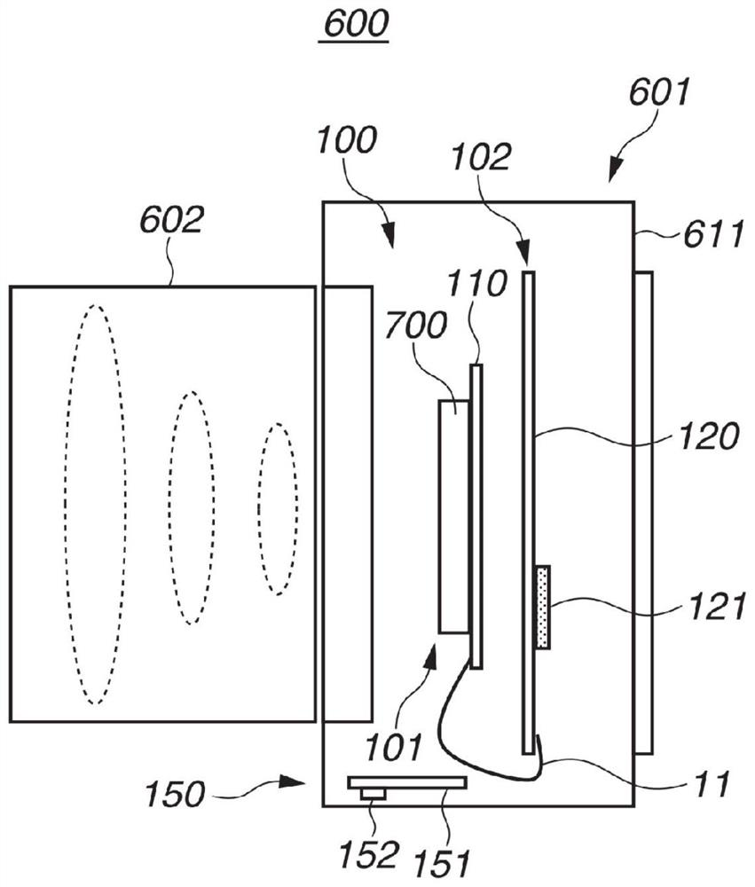
[0015] figure 1 is an explanatory diagram showing a digital camera 600 as an image capture device as an example of electronic equipment according to the first exemplary embodiment. A digital camera 600 as an image capturing device is a lens-interchangeable type digital camera and includes a camera body 601 . A lens unit (lens barrel) 602 including a lens can be detached from the camera body 601 . The camera body 601 includes a housing 611 and the image capturing unit 100 and the wireless communication unit 150 accommodated in the housing 611 .

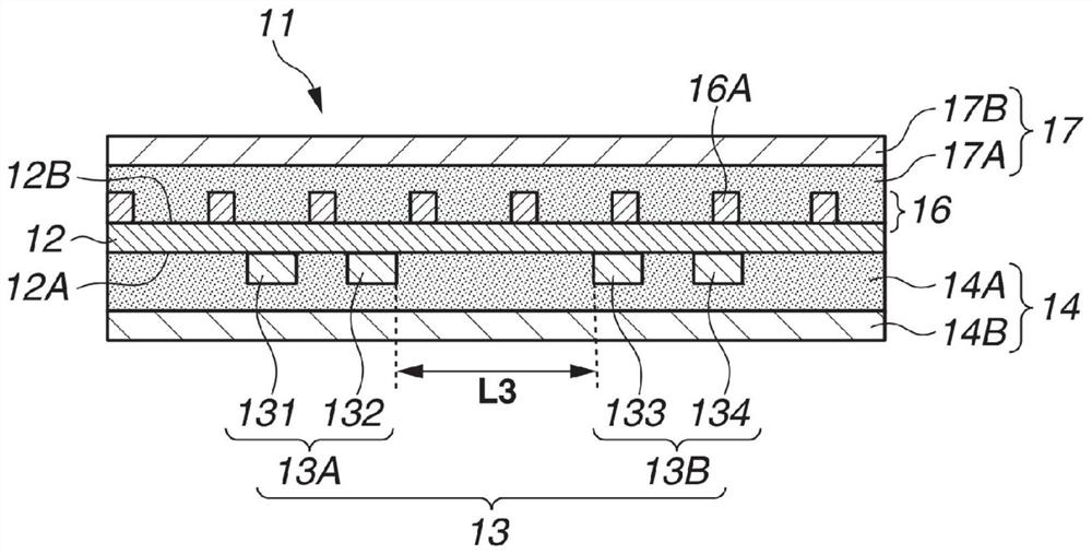
[0016] The image capture unit 100 includes a first printed circuit board 101, a second printed circuit board 102, and a flexible wiring board 11 as a wiring substrate (wiring substrate) that electrically connects the first printed circuit board 101 and the second printed circuit board 102. p...


PUM

PropertyMeasurementUnit
lengthaaaaaaaaaa
thicknessaaaaaaaaaa
thicknessaaaaaaaaaa

Abstract

The invention relates to a wiring substrate and an electronic device. The wiring substrate which includes a base member having a first surface, a first differential signal line disposed on the first surface of the base member and a second differential signal line disposed adjacent to the first differential signal line on the first surface of the base member. A ground layer which faces the first and second differential signal lines, has a plurality of openings continuously arranged along a predetermined direction. In a planar view of the wiring substrate, where a length of each of the plurality of openings in a direction along the signal lines is a length L1, a length of the opening in a direction orthogonal to L1 is a length L2, and a distance between the first and second differential signal lines is a length L3, L1 is equal to or greater than four times L2, and L2 is equal to or less than L3.

Description

technical field [0001] The present disclosure generally relates to wiring substrates for electronic devices, and particularly relates to techniques for reducing noise generated from wiring substrates. Background technique [0002] Two semiconductor devices in electronic equipment communicate data with each other using digital signals. Digital signals in data communications are usually transmitted via differential signal lines. Radiation noise generated by differential signal lines and crosstalk noise generated between differential signal lines may cause degradation of digital signal quality and failure of semiconductor devices. Japanese Patent Laid-Open No. 2000-077802 discusses a wiring substrate including a shield having a predetermined opening pattern for reducing radiation noise generated from differential signal lines. Contents of the invention [0003] A first aspect of the present disclosure provides a wiring substrate including: a base member having a first surfa...

Claims


Application Information

Patent Timeline
Patent Type & Authority Applications(China)
IPC IPC(8): H05K1/02
CPCH05K1/0219H01L27/14618H01L27/14625H05K1/0237H05K2201/09236H05K1/0225H05K2201/09681H05K1/148H05K2201/0154H05K1/0353H05K2201/0141H05K2201/0145H05K1/0224H05K1/0298H05K1/18H05K1/11H01L27/14636
Inventor 吉田季行小川优松本昇司
Owner CANON KK
Features
  • R&D
  • Intellectual Property
  • Life Sciences
  • Materials
  • Tech Scout
  • Unparalleled Data Quality
  • Higher Quality Content
  • 60% Fewer Hallucinations
Learn More