Pixel circuit, driving method thereof and display device
A pixel circuit and circuit technology, applied in static indicators, instruments, etc., can solve the problems of poor stability of micro-light-emitting diodes, reduce the display effect of the display panel, and cannot control the brightness and gray scale of micro-light-emitting diodes, so as to improve the display effect Effect
- Summary
- Abstract
- Description
- Claims
- Application Information
AI Technical Summary
Problems solved by technology
Method used
Image


Examples
Embodiment 1
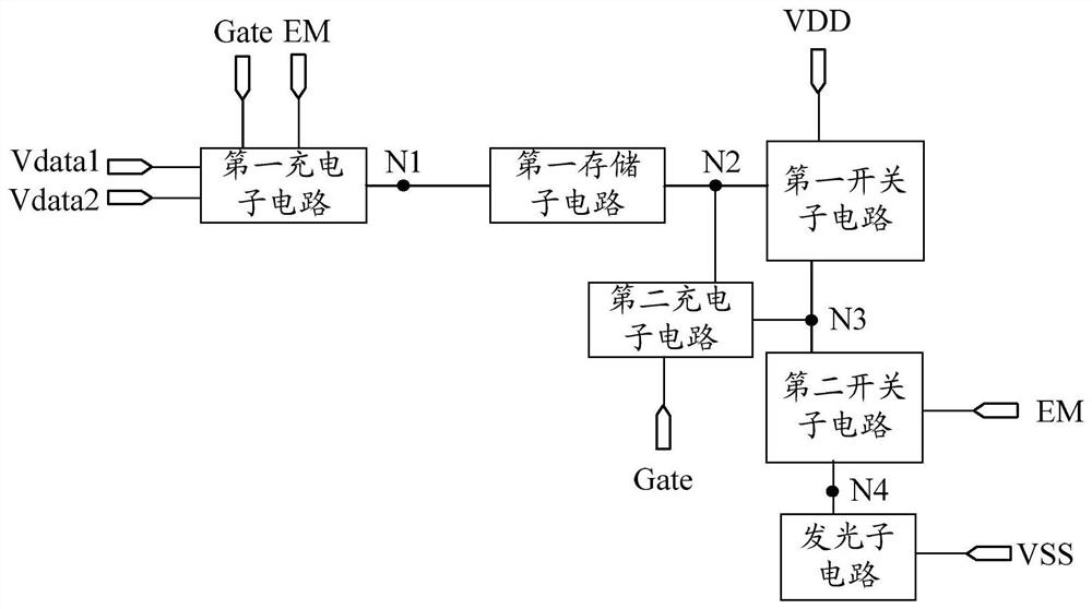
[0048] An embodiment of the present invention provides a pixel circuit, which is used for controlling the conduction duration of a current path between a first voltage terminal and a second voltage terminal. When the current path is turned on, the first voltage output from the first voltage terminal and the second voltage output from the second voltage terminal can provide a potential difference to the current path.
[0049] In this embodiment, the first voltage output from the first voltage terminal VDD may be a constant high level, and the second voltage output from the second voltage terminal VSS may be a constant low level.
[0050] figure 1 A schematic structural diagram of a pixel circuit provided for an embodiment of the present invention, such as figure 1 As shown, the pixel circuit includes: a first charging subcircuit, a second charging subcircuit, a first storage subcircuit, a first switching subcircuit, a second switching subcircuit and a light emitting subcircuit...
Embodiment 2
[0091] Based on the inventive concept of the above-mentioned embodiments, some embodiments of the present invention further provide a driving method for a pixel circuit, which is applied to the pixel circuit provided in the first embodiment above. In one image frame, the pixel circuit has multiple scanning periods.
[0092] In a scanning period (such as the first scanning period), the driving method of the pixel circuit, such as Figure 8 As shown, steps 100-101 are included.
[0093] Step 100, providing the first voltage to the first voltage terminal, providing the scanning signal to the scanning signal terminal, providing the first data voltage to the first data signal terminal, and writing the first data voltage to the first node through the first charging sub-circuit, The second charging sub-circuit compensates the second node under the control of the scanning signal terminal;
[0094] Specifically, when the second charging sub-circuit compensates the second node under th...
Embodiment 3
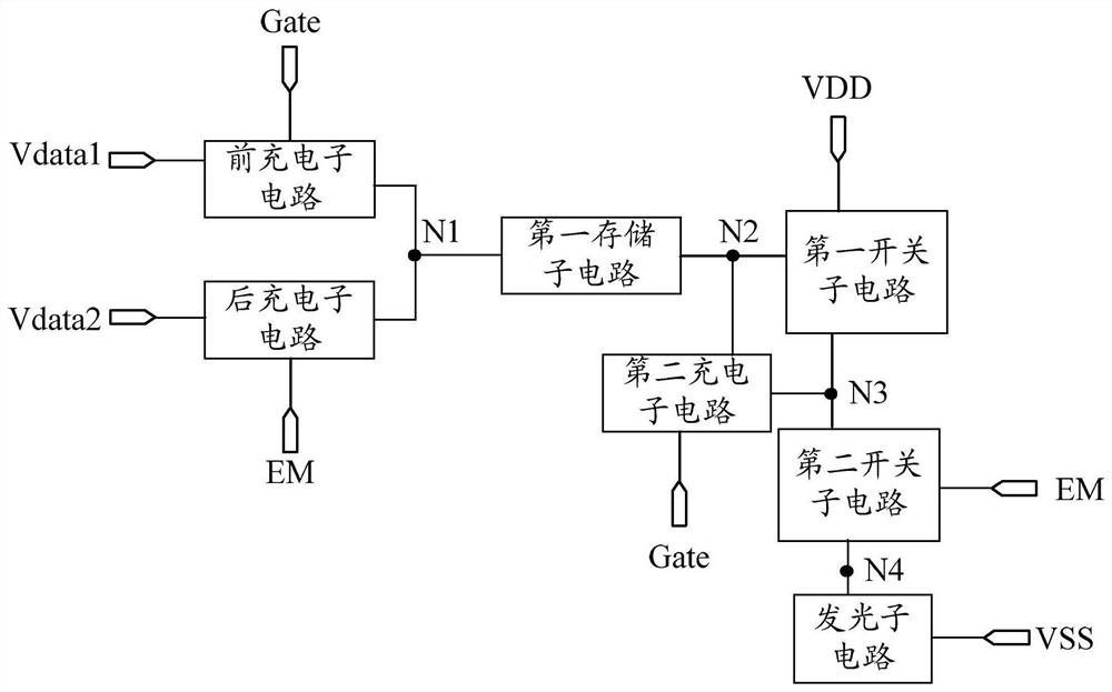
[0099] An embodiment of the present invention provides a pixel circuit, Figure 9 It is a structural schematic diagram of the third embodiment of the pixel circuit of the present application. This embodiment is an extension of the aforementioned first embodiment. The main structure is basically the same as that of the aforementioned first embodiment. The difference is that the first embodiment of this embodiment The switch sub-circuit is respectively connected to the third voltage terminal Vref, the second node N2 and the third node N3, and is used to provide the signal of the third voltage terminal Vref to the third node N3 under the control of the second node N2. For example, the control terminal of the first switch subcircuit is connected to the second node N2, the first terminal of the first switch subcircuit is connected to the third voltage terminal Vref, and the second terminal of the first switch subcircuit is connected to the third node N3. The pixel circuit in this e...
PUM
 Abstract
Description
Claims
Application Information
 - Generate Ideas
- Intellectual Property
- Life Sciences
- Materials
- Tech Scout
- Unparalleled Data Quality
- Higher Quality Content
- 60% Fewer Hallucinations
Browse by: Latest US Patents, China's latest patents, Technical Efficacy Thesaurus, Application Domain, Technology Topic, Popular Technical Reports.
© 2025 PatSnap. All rights reserved.Legal|Privacy policy|Modern Slavery Act Transparency Statement|Sitemap|About US| Contact US: help@patsnap.com