
Manufacturing method of display panel, display panel and to-be-cut display panel

A technology for display panels and manufacturing methods, applied in semiconductor/solid-state device manufacturing, semiconductor devices, electrical components, etc., can solve the problems of display panel line damage and low yield rate of display panels, and achieve low manufacturing yield and avoid Static damage and the effect of improving manufacturing yield

Active Publication Date: 2021-07-02
HEFEI XINSHENG OPTOELECTRONICS TECH CO LTD +1
View PDF7 Cites 1 Cited by
  • Summary
  • Abstract
  • Description
  • Claims
  • Application Information

AI Technical Summary

Problems solved by technology

[0004] However, in the above method, after removing the static electricity protection circuit and the source-drain conductive pattern in the preset cutting area, when other structures are subsequently formed, the generated static electricity may damage the lines in the display panel, which in turn may cause the display panel to be damaged. low yield

Method used


Image

  • Manufacturing method of display panel, display panel and to-be-cut display panel
  • Manufacturing method of display panel, display panel and to-be-cut display panel
  • Manufacturing method of display panel, display panel and to-be-cut display panel

Examples


Embodiment Construction

[0081] In order to make the purpose, technical solution and advantages of the present application clearer, the implementation manners of the present application will be further described in detail below in conjunction with the accompanying drawings.

[0082] At present, display panels of different sizes are usually manufactured by different mask plates, for example, a 55-inch display panel is manufactured by a 55-inch matching mask plate, and a 49-inch display panel is manufactured by a 49-inch matching mask plate. manufacturing, so that display panels of various sizes can be manufactured.

[0083] However, there are many structures in the display panel, and each structure requires different masks to be manufactured, so that a display panel of each size needs to be manufactured with a set of masks including a plurality of mask boards, resulting in the design It takes a long time to manufacture the mask plate, and the cost is relatively high.

[0084] In one way, a display pan...


PUM


Abstract

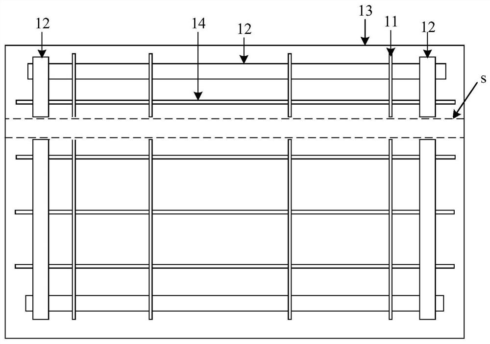
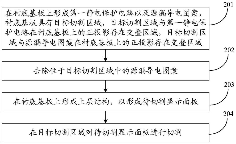
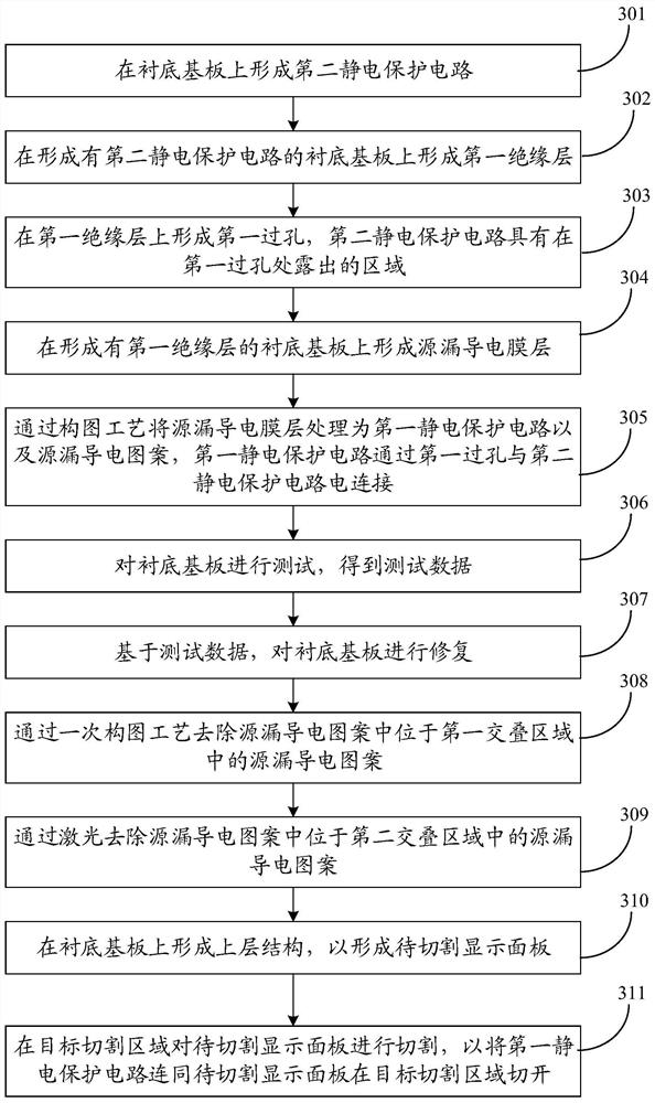
The invention discloses a manufacturing method of a display panel, the display panel and a to-be-cut display panel, and belongs to the technical field of display. The method comprises the following steps: forming a first electrostatic protection circuit and a source-drain conductive pattern on a substrate; removing the source-drain conductive pattern in the target cutting area; forming an upper layer structure on the substrate so as to form a to-be-cut display panel; and cutting the to-be-cut display panel in the target cutting area. When the internal structure of the display panel is manufactured, only the source-drain conductive pattern in the target cutting area is removed, and the electrostatic protection circuit in the target cutting area is reserved, so that the electrostatic protection circuit can play a role in electrostatic protection all the time in the process of forming the internal structure of the display panel; the manufacturing yield of the display panel is improved, the problem that the manufacturing yield of the display panel is low in the prior art can be solved, and the effect of improving the manufacturing yield of the display panel is achieved.

Description

technical field [0001] The present application relates to the field of display technology, in particular to a method for manufacturing a display panel, a display panel and a display panel to be cut. Background technique [0002] A display panel is a device with a display function. There are various sizes of display panels, and display panels of different sizes are usually manufactured using different masks. In order to reduce the number of mask plates, one way is to manufacture a display panel through a set of mask plates, and then cut the display panel to realize the manufacture of display panels of various sizes. [0003] In a method for manufacturing a display panel, after forming an electrostatic protection circuit and a source-drain conductive pattern of the same layer on a base substrate, the electrostatic protection circuit and the source-drain conductive pattern in a preset cutting area are removed through a patterning process, In order to avoid failure of the circ...

Claims


Application Information

Patent Timeline
IPC IPC(8): H01L27/12H01L21/77
CPCH01L27/124H01L27/1259
Inventor 王海涛王明成军周斌汪军黄勇潮苏同上王庆贺
Owner HEFEI XINSHENG OPTOELECTRONICS TECH CO LTD
Learn More