Array substrate and manufacturing method

A technology of an array substrate and a manufacturing method, which is applied in the field of liquid crystal display, can solve problems such as short circuit of the array substrate, and achieve the effect of avoiding electrostatic damage

Inactive Publication Date: 2014-11-05
TCL CHINA STAR OPTOELECTRONICS TECH CO LTD
View PDF6 Cites 12 Cited by
  • Summary
  • Abstract
  • Description
  • Claims
  • Application Information

AI Technical Summary

Problems solved by technology

[0003] The purpose of the present invention is to provide an array substrate to solve the technical problem of short ci

Method used


Image

  • Array substrate and manufacturing method
  • Array substrate and manufacturing method

Examples


Embodiment Construction

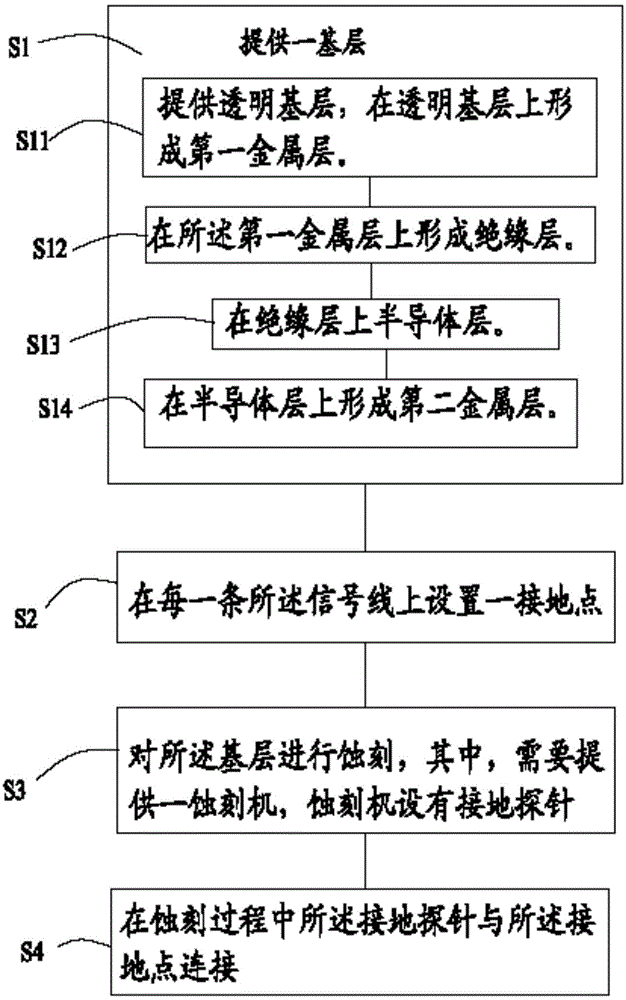
[0023] The following will clearly and completely describe the technical solutions in the embodiments of the present invention with reference to the accompanying drawings in the embodiments of the present invention. Obviously, the described embodiments are only some, not all, embodiments of the present invention. Based on the embodiments of the present invention, all other embodiments obtained by persons of ordinary skill in the art without creative efforts fall within the protection scope of the present invention.

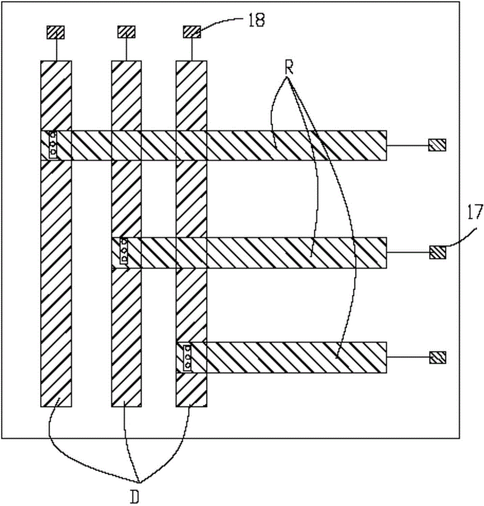
[0024] see figure 1 A preferred embodiment of the present invention provides an array substrate, the base layer of the array substrate is provided with a plurality of parallel signal lines D and a parallel test line R corresponding to each signal line D; the test line R The plurality of signal lines D are located on different surfaces of the array substrate and arranged crosswise; one end of the test wiring R is connected to the corresponding signal line D, and the...


PUM


Abstract

The invention provides an array substrate which comprises a base layer. A plurality of signal lines parallel to one another and test wires are arranged in the base layer, the test wires correspond to the signal lines respectively and are parallel to one another, the test wires and the signal lines are located on different surface layers of the base layer and are crossed, one end of each test wire is connected with the corresponding signal line, the other end of each test wire is connected with a test point, and each signal line is connected with an earth point. The invention further provides a manufacturing method of the array substrate.

Description

technical field [0001] The invention relates to liquid crystal display technology, in particular to an array substrate and a manufacturing method. Background technique [0002] A Liquid Crystal Display (LCD for short) displays various images by controlling the light transmittance of liquid crystal pixels arranged in an array on a liquid crystal panel. Generally, a driver chip for driving a liquid crystal panel is crimped on a thin film transistor liquid crystal display (Thin Film Transistor Liquid Crystal Display; TFT LCD for short) panel. Among them, the array substrate forms a plurality of signal lines in the manufacturing process, and before cutting the array substrate to form a TFT array substrate or installing a driving circuit module on the liquid crystal display panel, it is necessary to conduct electrical tests on the signals of the array substrate, etc., to detect failures. For an array substrate that works normally, a common detection method is to set a test line ...

Claims


Application Information

Patent Timeline
IPC IPC(8): G02F1/1362
Inventor 付延峰
Owner TCL CHINA STAR OPTOELECTRONICS TECH CO LTD
Why Eureka
Try Eureka