
Substrate for semiconductor device, manufacturing method thereof, semiconductor device, and frame main body

Inactive Publication Date: 2002-12-26
SONY CORP
View PDF20 Cites 0 Cited by
  • Summary
  • Abstract
  • Description
  • Claims
  • Application Information

AI Technical Summary

Benefits of technology

[0020] A further object is to provide a manufacturing method for manufacturing the substrate for semiconductor device, which is capable of effectively preventing the semiconductor device from the electrostatic damage.
[0023] With this configuration, even if the end faces of the substrate for semiconductor device is electrostatically charged by friction with the transfer unit or the chucking unit during transfer or during chucking, no discharge current flows through the wiring for surface treatment because no end of the wiring for surface treatment comes into contact with the transfer unit or the chucking unit. Therefore, even for a semiconductor chip of an LGA or BGA type, or the like, which tends to undergo electrostatic damage, it is possible to effectively protect the semiconductor chip from damage by static electricity (electrostatic damage).
[0025] According to this aspect of the invention, when the semiconductor chip of the above aspect is charged, discharge occurs from the semiconductor chip via the wiring for power supply or grounding. As a result, it is possible to prevent the semiconductor chip from electrostatic damage.
[0029] In accordance with such the manufacturing method including the steps of cutting the wiring for the surface treatment by slitting it, or the like, after a surface treatment, ends of the wiring for surface treatment may be exposed at the side surfaces of the insulating substrate body. Since, if so, the internal wiring for surface treatment is electrically disconnected, no discharge current of static electricity flows through the semiconductor chip via the wiring for surface treatment. As a result, there is no risk that the semiconductor chip will be damaged by static electricity.
[0033] By doing as described above, it is possible to provide the substrate for semiconductor device resistant to electrostatic damage. Further, by using the substrate for a semiconductor device, it is possible to provide a semiconductor device resistant to electrostatic damage.

Problems solved by technology

By such a repetition of charging and discharging, the semiconductor chip may be damaged by static electricity.
Therefore, such the semiconductor device is susceptible to static electricity.
As a result, the semiconductor element in the semiconductor device has a high possibility of undergoing electrostatic damage (ESD damage) also due to slight charging and discharging.
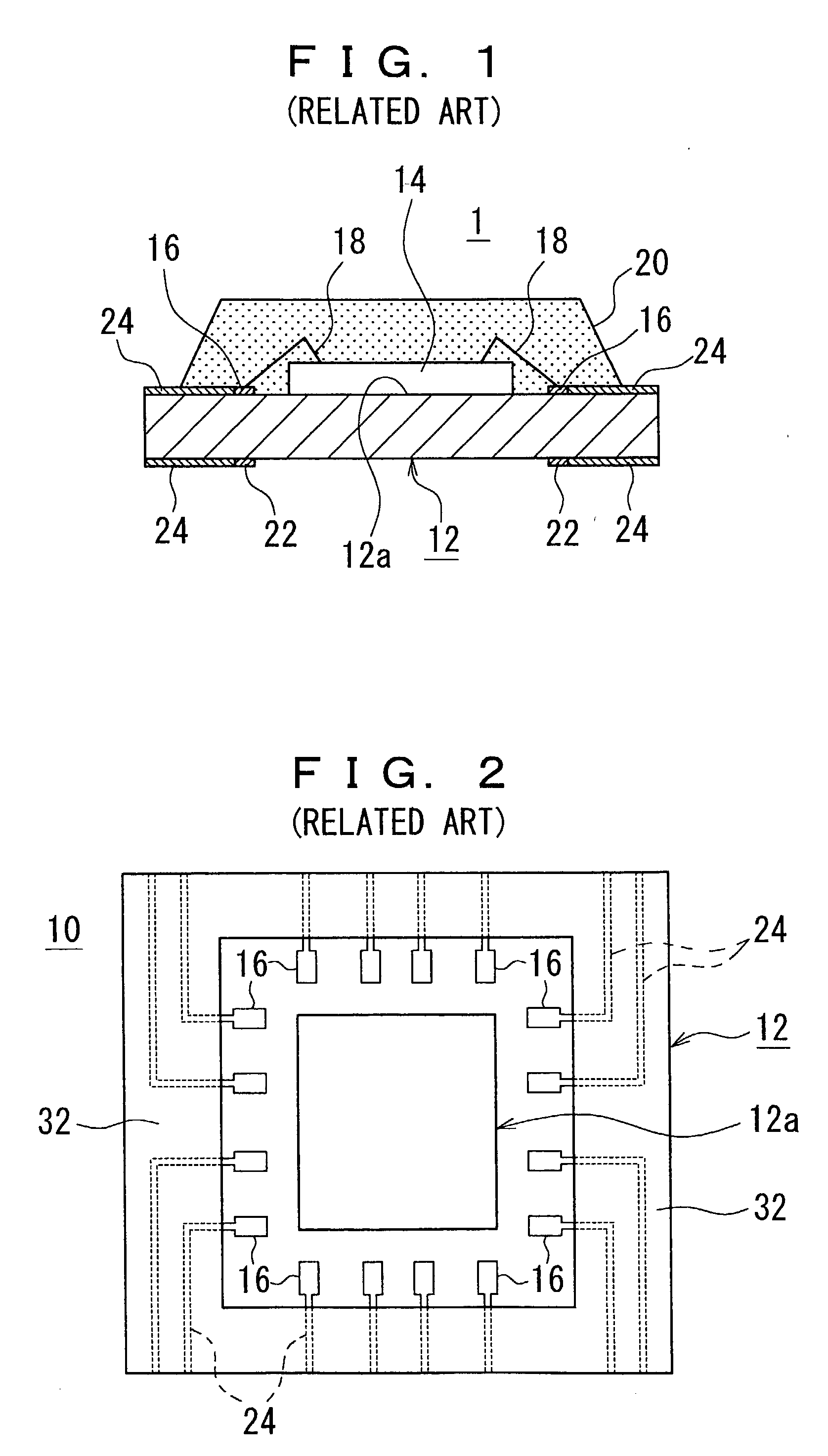
Friction occurs due to the rubbing of the wiring for surface treatment to be used for surface treatment against a transfer block or a chucking block.
Therefore, the wiring for connecting the bonding electrodes and the external electrodes cannot extend to the side surfaces of the insulating substrate body.

Method used


Image

  • Substrate for semiconductor device, manufacturing method thereof, semiconductor device, and frame main body
  • Substrate for semiconductor device, manufacturing method thereof, semiconductor device, and frame main body
  • Substrate for semiconductor device, manufacturing method thereof, semiconductor device, and frame main body

Examples


Embodiment Construction

)

[0050] Subsequently, preferred embodiments of a substrate for semiconductor device, a manufacturing method for manufacturing the same, a semiconductor device, and a frame main body in accordance with this invention will be described in detail by reference to the drawings.

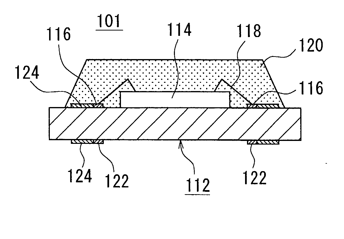
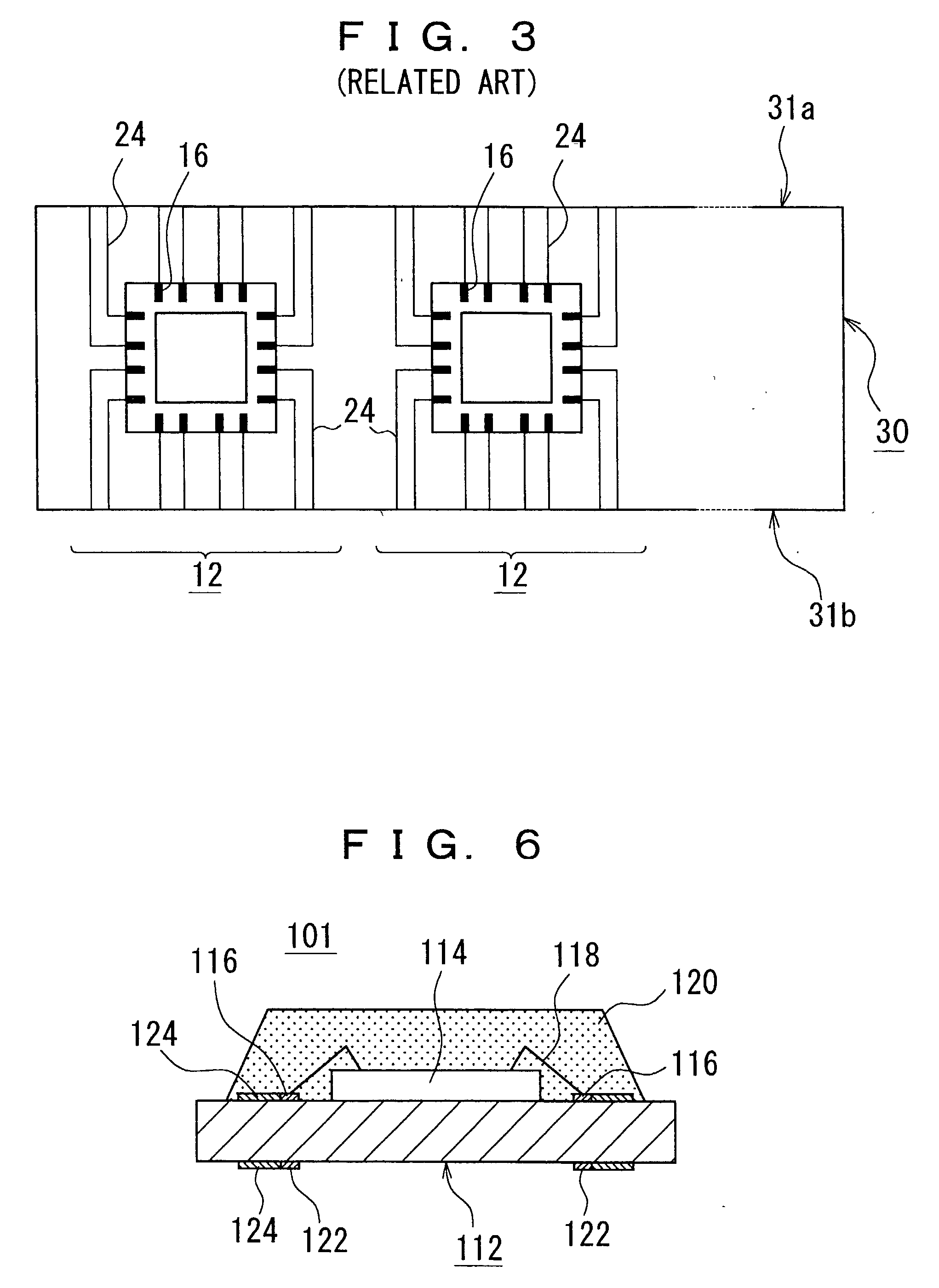
[0051] FIG. 5 shows an embodiment of a lead frame 100 to be used as the substrate for semiconductor device in accordance with this invention. FIG. 6 is a cross sectional view of the semiconductor device 101 in accordance with this invention using this lead frame 100. FIG. 7 shows a frame main body 103, which is to be segmented into each lead frame 100 of FIG. 5.

[0052] A description will be given by reference to FIGS. 5 to 7. According to the embodiment of this invention, the lead frame 100 comprises a lead frame body 112, which is insulating substrate body. The lead frame 100 also comprises a die pad 112a in rectangle form for mounting and fixing a semiconductor chip 114 on the one surface (top surface) of a lead f...


PUM


Abstract

A lead frame comprises lead frame body having cut-away portions cut away from the side surfaces of the lead frame body, die pad for securing semiconductor chip, bonding electrodes surrounding the die pad, external electrodes for allowing the lead frame to be mounted, wiring for surface treatment extending on the lead frame body with its end being located at a portion of each of the side surfaces of the lead frame body, the portion being opposed the cut-away portions. The bonding electrode and the wiring for surface treatment as well as the external electrode and the wiring for surface treatment are electrically connected, respectively. Even when the lead frame is electrostatically charged by friction with a transfer unit, the semiconductor chip on the lead frame avoids the electrostatic damage.

Description

[0001] 1. Field of the Invention[0002] The present invention relates generally to a substrate for semiconductor device, a manufacturing method thereof, a semiconductor device, and a frame main body. More particularly, it relates to the substrate for semiconductor device and the like wherein an insulating substrate body for mounting the semiconductor device has a cut-away portion cut away from a side surface thereof and wiring for surface treatment extends on the insulating substrate body with an end thereof gathering in a portion of a side surface of the insulating substrate body, the portion being opposed the cut-away portion, thereby preventing the wiring for surface treatment from extending through the side surface of the insulating substrate body so that even when the substrate gets static electricity during the transfer thereof, the semiconductor chip can avoid an electrostatic damage.[0003] 2. Description of Related Art[0004] In recent years, there have been demands for higher...

Claims


Application Information

Patent Timeline
IPC IPC(8): H01L23/13H01L23/12H01L23/50H01L23/62H05K3/24
CPCH01L23/13H01L23/62H01L2224/48227H01L24/48H01L2224/45144H01L2924/12041H01L2924/00014H01L2924/00H01L2924/181H01L24/45H01L2924/00012H01L2224/45015H01L2924/207H01L23/50
Inventor TOGAWA, MIYOSHI
Owner SONY CORP
Learn More