Fingerprint Sensor Having ESD Protection Structure

A technology for electrostatic protection and electrostatic protection electrodes, which is applied in the field of fingerprint sensors with electrostatic protection structures, can solve the problems of decreased fingerprint sensing accuracy and damage to the sensing electrode plate 61, etc., and achieves the effect of avoiding electrostatic damage.

Inactive Publication Date: 2016-10-19
ELAN MICROELECTRONICS CORPORATION
View PDF8 Cites 1 Cited by
  • Summary
  • Abstract
  • Description
  • Claims
  • Application Information

AI Technical Summary

Problems solved by technology

[0004] However, since the conductive grid 70 is coplanar with the plurality of sensing electrode plates 61, the distance between the finger 90 and the conductive grid 70 and the sensing electrode plates 61 is close, and excessive static electricity has no time to pass through the grounded conductive grid 70 When leaking, the sensing electrode plate 61 may be damaged, resulting in a decrease in the accuracy of fingerprint sensing

Method used


Image

  • Fingerprint Sensor Having ESD Protection Structure
  • Fingerprint Sensor Having ESD Protection Structure
  • Fingerprint Sensor Having ESD Protection Structure

Examples


Embodiment Construction

[0035] Below in conjunction with accompanying drawing, structural principle and working principle of the present invention are specifically described:

[0036] The present invention provides an electrostatic protection structure for the fingerprint sensor to prevent the fingerprint sensor from being damaged by static electricity. The following embodiments illustrate the structure of the fingerprint sensor of the present invention.

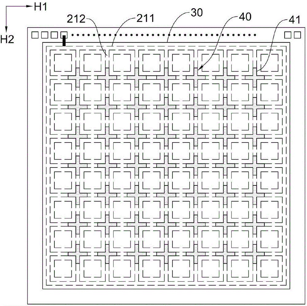
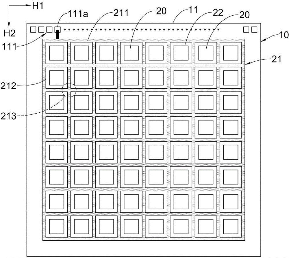
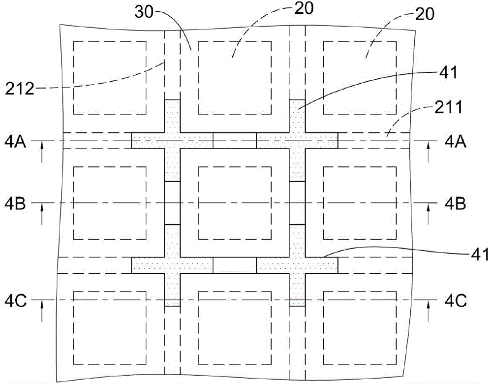
[0037] See first figure 1 , figure 2 and Figure 4A Shown is the first preferred embodiment of the fingerprint sensor 10 of the present invention, which includes a substrate 11, a plurality of sensing electrode plates 20, a first conductive layer 21, a dielectric layer 30, and a second conductive layer 40 and a protective layer 50.

[0038] The plurality of sensing electrode plates 20 are arranged on an upper surface of the substrate 11, and an accommodation space 22 is formed between the plurality of sensing electrode plates 20; in this embod...


PUM


Abstract

The invention discloses a fingerprint sensor having an ESD protection structure having multiple sensing electrode plates formed on a substrate and defining a receiving space among the sensing electrode plates; an ESD protection electrode part connected to ground and having a first conductive layer and a second conductive layer, wherein the first conductive layer is coplanar with the sensing electrode plates, and the second conductive layer is formed on the substrate and the second conductive layer has multiple conductive elements separated to each other; a dielectric layer; and a protection layer. The conductive pieces are overlapped with the first conductive layer in a vertical direction and are electrically connected to the first conductive layer through formed on the conductive layer. When the first conductive layer and / or the second conductive layer is coupled to ground, both of the first and second conductive layers provide a discharging path of static electricity.

Description

technical field [0001] The invention relates to a fingerprint sensor, in particular to a fingerprint sensor with an electrostatic protection structure. Background technique [0002] Currently, a chip-type fingerprint sensor disclosed in US Patent No. 5,325,442, please refer to Figure 9 and Figure 10 As shown, its structure mainly forms a sensing electrode layer 60 on a semiconductor substrate 80 first, and then covers the sensing electrode layer 60 with a protection layer 81 . The semiconductor substrate 80 forms a sensing integrated circuit (not shown) electrically connected to the sensing electrode layer 60, and the sensing electrode layer 60 includes a plurality of sensing electrode plates 61 arranged in a matrix. When the finger 90 touches or approaches The protective layer 81, the finger 90 and each of the sensing electrode plates 61 will form a plate capacitance Cf. Therefore, the sensing integrated circuit measures the sensing signal of each of the sensing electrod...

Claims


Application Information

Patent Timeline
IPC IPC(8): G06K9/00
Inventor 江宗殷王俊淇唐春安
Owner ELAN MICROELECTRONICS CORPORATION
Why Eureka
Try Eureka