Wafer-level packaging reliability optimization method

A wafer-level packaging and optimization method technology, applied in the direction of instruments, electrical digital data processing, electrical components, etc., can solve the problems of large number of experiments and low efficiency, and achieve the effect of improving thermal fatigue life and thermal fatigue life

Pending Publication Date: 2021-07-16
NANTONG UNIVERSITY
View PDF4 Cites 0 Cited by
  • Summary
  • Abstract
  • Description
  • Claims
  • Application Information

AI Technical Summary

Problems solved by technology

The disadvantage of this method is that for samples with multiple factors and multiple values, if full factor analysis is performed, the number of experiments is large and the efficiency is low

Method used


Image

  • Wafer-level packaging reliability optimization method
  • Wafer-level packaging reliability optimization method
  • Wafer-level packaging reliability optimization method

Examples


Embodiment Construction

[0033] The technical solutions in the embodiments of the invention will be clearly and completely described below in conjunction with the accompanying drawings in the embodiments of the invention. Obviously, the described embodiments are only part of the embodiments of the invention, not all of them. example. Based on the embodiments of the present invention, all other embodiments obtained by persons of ordinary skill in the art without making creative efforts belong to the scope of protection of the present invention.

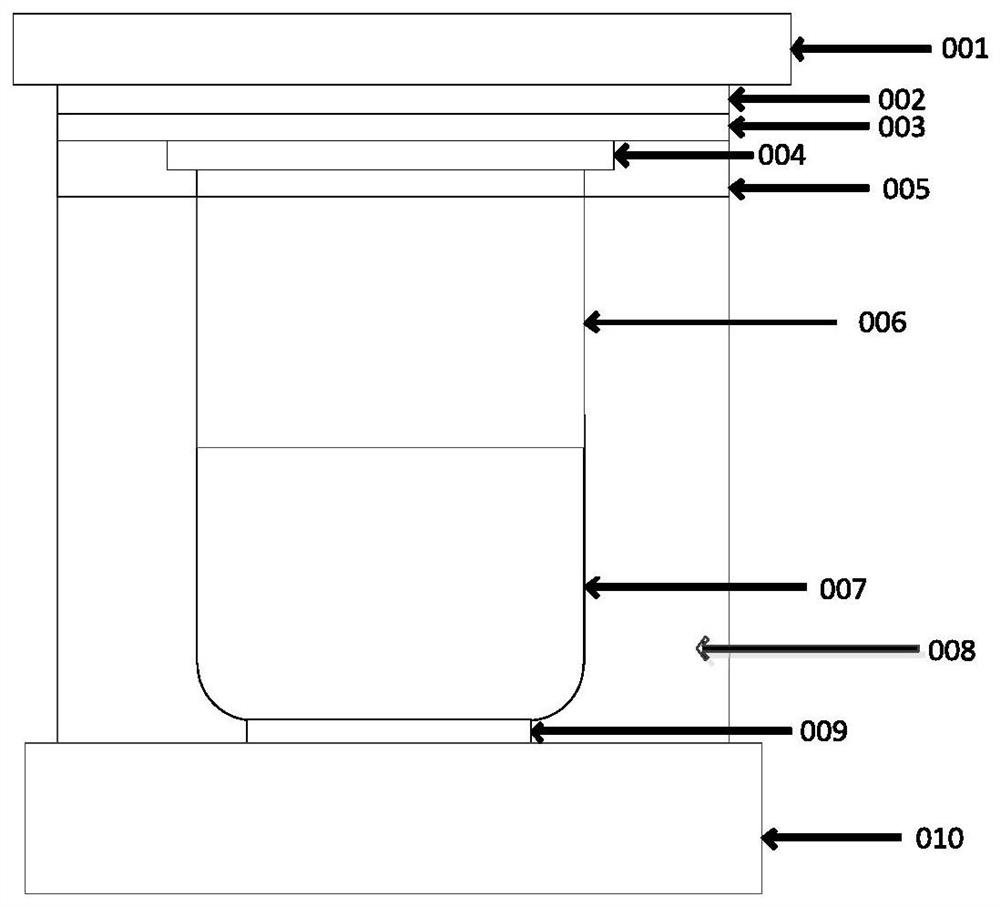
[0034] On the one hand, if figure 1 As shown, the present invention provides a fine-pitch copper pillar wafer-level packaging structure:

[0035] A wafer-level packaging structure of fine-pitch copper pillars, comprising:

[0036] Printed circuit board 010;

[0037] The pad 009 is arranged on the printed circuit board 010;

[0038] The solder joint 007 is set on the pad 009;

[0039] Copper pillar 006, set on solder joint 007;

[0040] The redistribution...


PUM


Abstract

The invention provides a wafer-level packaging reliability optimization method. The method comprises the following steps: obtaining initial thermal fatigue life of a packaging structure according to the initial structure size of the packaging structure and welding spot material simulation; selecting factors influencing the fatigue life of the packaging structure, and forming a proper orthogonal table; and simulating optimal combination of each factor to obtain the thermal fatigue life, and comparing the thermal fatigue life of the optimized structure with the thermal fatigue life of the initial structure to find that the thermal fatigue life is obviously increased and the reliability of the packaging structure is optimized.

Description

[0001] This invention is a divisional application of application number 201911276819X, application date December 12, 2019, applicant: Nantong University, invention name: a fine-pitch copper pillar wafer-level packaging structure and reliability optimization method. technical field [0002] The invention relates to the technical field of chip packaging, in particular to a micro-pitch copper pillar wafer-level packaging structure and a reliability optimization method. Background technique [0003] Due to the rapid development of portable electronic equipment and mobile communication devices, new and higher requirements have been put forward in terms of electrical performance and heat dissipation performance. Wafer-level packaging technology, as the latest revolutionary packaging technology, caters well to the needs of this era and has been more and more widely used. However, due to the thermal expansion coefficient mismatch between the chip and the printed circuit board (PCB),...

Claims


Application Information

Patent Timeline
Patent Type & Authority Applications(China)
IPC IPC(8): G06F30/398H01L23/498H05K1/11G06F113/18G06F119/02G06F119/04G06F119/08
CPCH01L23/49811H01L23/49838H05K1/115G06F30/398G06F2113/18G06F2119/02G06F2119/04G06F2119/08
Inventor 孙海燕高波金玲玥赵继聪孙玲
Owner NANTONG UNIVERSITY
Why Eureka
Try Eureka