

A semiconductor graphene nanoribbon and its preparation method and application
A graphene nanobelt and semiconductor technology, applied in graphene, semiconductor devices, nano-carbon, etc., can solve the problems of opening and inability to apply semiconductor devices, etc., and achieve the effect of simple production process route, good uniformity and high product quality
- Summary
- Abstract
- Description
- Claims
- Application Information
AI Technical Summary
Problems solved by technology
Method used
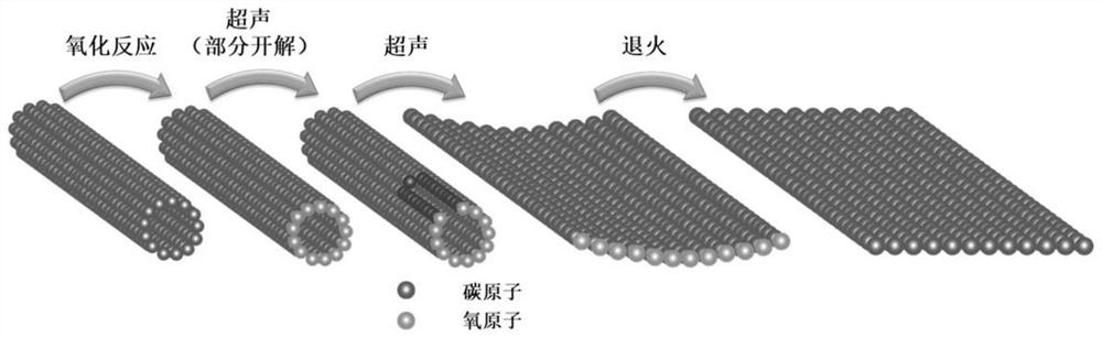
Image

Examples
Embodiment 1
[0052] A preparation method of semiconductor graphene nanoribbon, comprising steps as follows:
[0053] (1) Preparation of single-walled carbon nanotube suspension:
[0054] 50 mg of single-walled carbon nanotubes with a diameter of 1.3 nm were annealed in air at 300 ° C for 30 minutes to effectively remove the amorphous carbon mixed therein; then the annealed single-walled carbon nanotubes were added to 50 mL concentrated sulfuric acid with a mass fraction of 98 wt%, and stirred for 2 hours to obtain a suspension of single-walled carbon nanotubes.
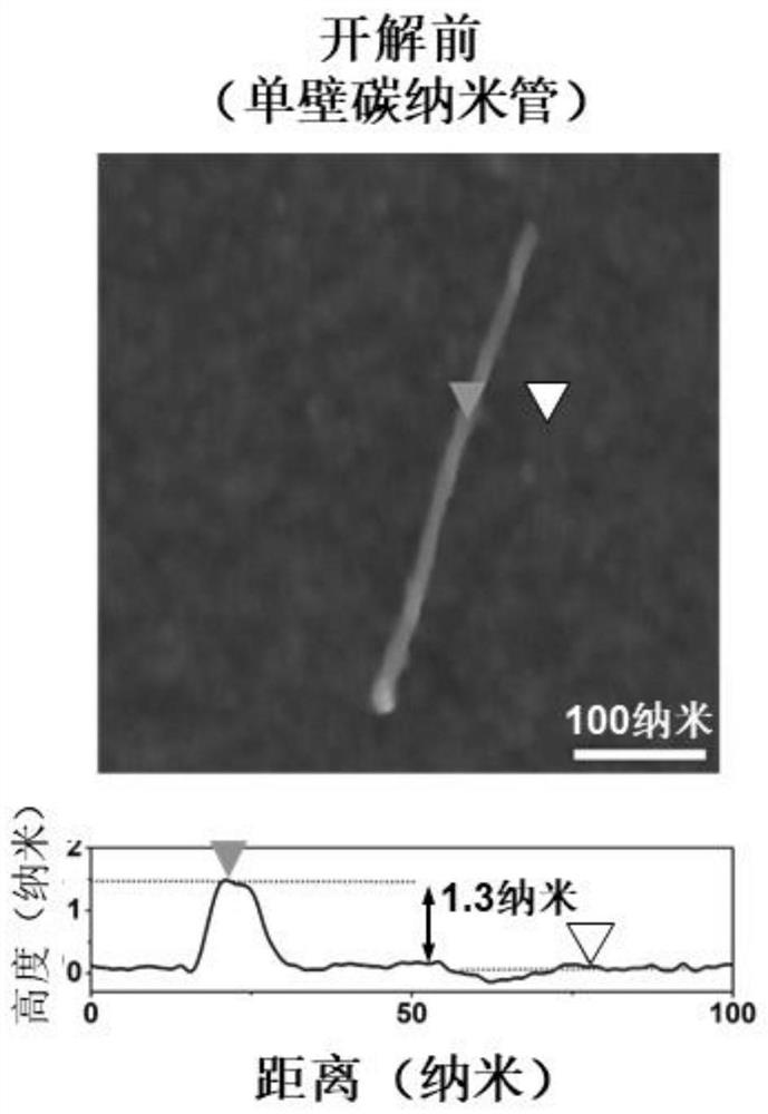
[0055] The atomic force microscope photo of the single-walled carbon nanotubes used in this step is as follows: figure 2 shown, from figure 2 As can be seen in , the single-walled carbon nanotubes used have a diameter of 1.3 nm.
[0056] (2) Preparation of single-walled carbon nanotubes with defects:
[0057] 25 mg of potassium permanganate was gradually added to the single-walled carbon nanotube suspension obtained in step ...
Embodiment 2
[0068] A preparation method of semiconductor graphene nanoribbon, comprising steps as follows:
[0069] (1) Preparation of single-walled carbon nanotube suspension:
[0070] 50 mg of single-walled carbon nanotubes with a diameter of 1.3 nm were annealed in air at 300 ° C for 60 minutes to effectively remove the amorphous carbon mixed therein; then the annealed single-walled carbon nanotubes were added to 100 mL concentrated sulfuric acid with a mass fraction of 98 wt%, and stirred for 2 hours to obtain a suspension of single-walled carbon nanotubes.
[0071] (2) Preparation of single-walled carbon nanotubes with defects:
[0072] Gradually add 25 mg of potassium permanganate to the single-walled carbon nanotube suspension obtained in step (1), and react at 45° C. for 60 minutes; after the reaction is completed, pour the resulting reaction solution into 400 mL of ice water, and then The single-walled carbon nanotubes with defects were obtained by filtering with an ethylene fi...
Embodiment 3
[0078] A preparation method of semiconductor graphene nanoribbon, comprising steps as follows:
[0079] (1) Preparation of single-walled carbon nanotube suspension:
[0080] 50 mg of single-walled carbon nanotubes with a diameter of 1.3 nm were annealed in air at 350 ° C for 60 minutes to effectively remove the amorphous carbon mixed therein; then the annealed single-walled carbon nanotubes were added to 100 mL concentrated sulfuric acid with a mass fraction of 98 wt%, and stirred for 2 hours to obtain a suspension of single-walled carbon nanotubes.
[0081] (2) Preparation of single-walled carbon nanotubes with defects:
[0082] Gradually add 25 mg of potassium permanganate to the single-walled carbon nanotube suspension obtained in step (1), and react at 60° C. for 30 minutes; after the reaction is completed, pour the resulting reaction solution into 800 mL of ice water, and then The single-walled carbon nanotubes with defects were obtained by filtering with an ethylene fi...
PUM
| Property | Measurement | Unit |
|---|---|---|
| diameter | aaaaa | aaaaa |
| diameter | aaaaa | aaaaa |
| thickness | aaaaa | aaaaa |
Abstract
Description
Claims
Application Information