Supercharge Your Innovation With Domain-Expert AI Agents!

Semiconductor processing equipment and control method of semiconductor processing equipment

A technology of process equipment and semiconductors, applied in the direction of program control design, program control device, resource allocation, etc., can solve problems such as prone to failure and low control efficiency

Pending Publication Date: 2021-07-27
BEIJING NAURA MICROELECTRONICS EQUIP CO LTD
View PDF0 Cites 0 Cited by
  • Summary
  • Abstract
  • Description
  • Claims
  • Application Information

AI Technical Summary

Problems solved by technology

[0005] The purpose of the embodiment of the present application is to provide a semiconductor process equipment and a control method for the semiconductor process equipment to solve the problems of low control efficiency and prone to failure of the existing semiconductor process equipment

Method used


Image

  • Semiconductor processing equipment and control method of semiconductor processing equipment
  • Semiconductor processing equipment and control method of semiconductor processing equipment
  • Semiconductor processing equipment and control method of semiconductor processing equipment

Examples


Embodiment Construction

[0023] Embodiments of the present application provide a semiconductor process equipment and a control method for the semiconductor process equipment, which are used to solve the problems of low control efficiency and easy failure of existing semiconductor process equipment.

[0024] In order to enable those skilled in the art to better understand the technical solutions in the present application, the technical solutions in the embodiments of the present application will be clearly and completely described below in conjunction with the drawings in the embodiments of the present application. Obviously, the described The embodiments are only some of the embodiments of the present application, but not all of them. Based on the embodiments in this application, all other embodiments obtained by persons of ordinary skill in the art without creative efforts shall fall within the scope of protection of this application.

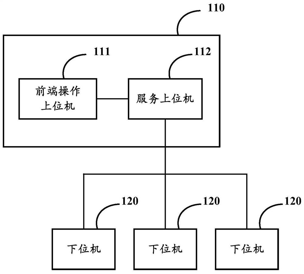
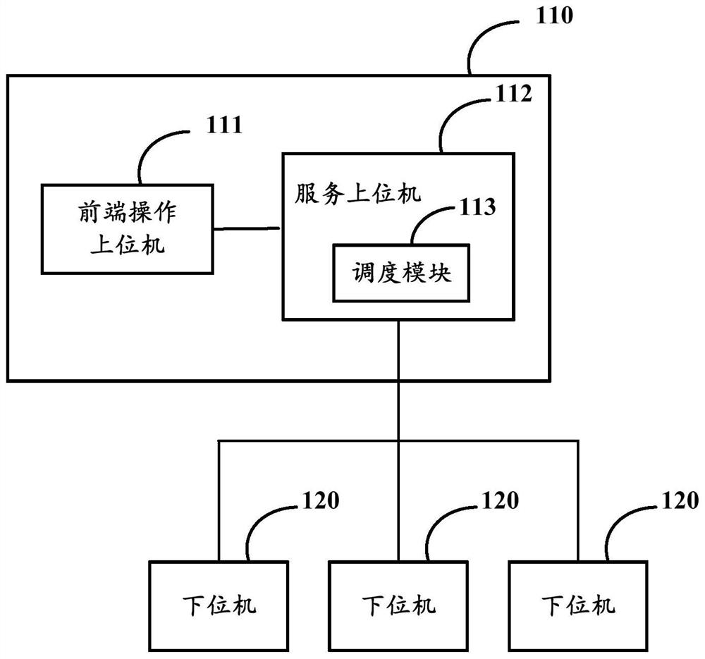
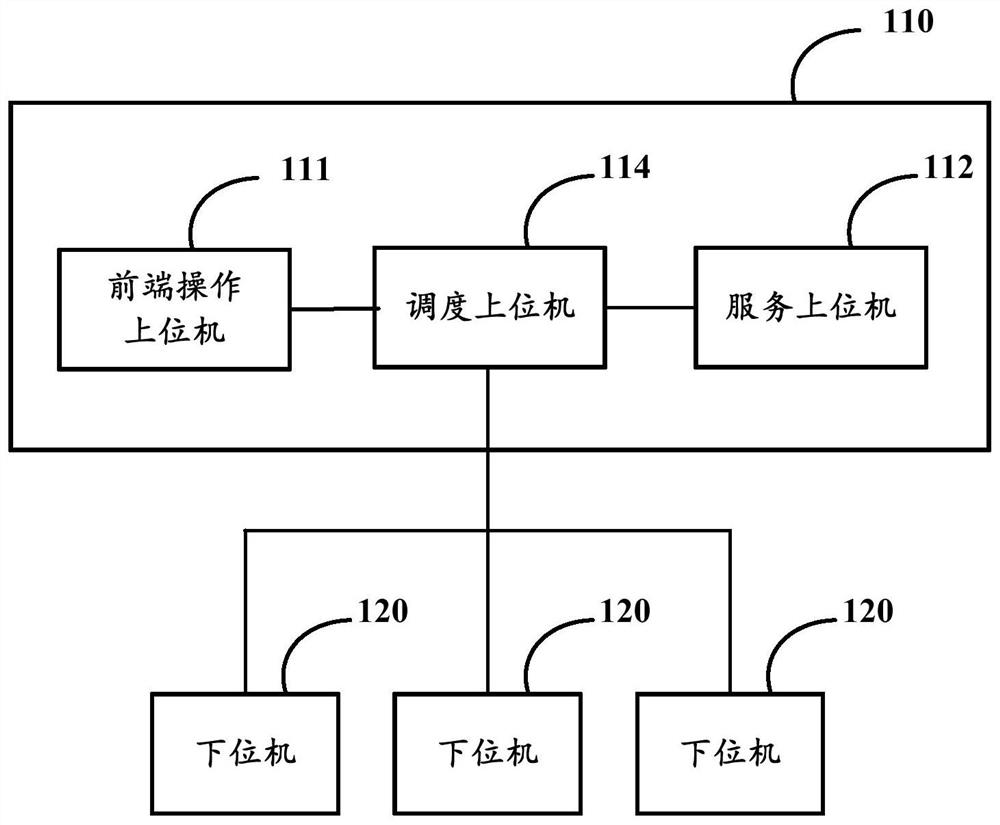
[0025] figure 1 is a schematic block diagram of a semiconducto...


PUM


Abstract

The embodiment of the invention discloses semiconductor process equipment and a control method of the semiconductor process equipment. The semiconductor process equipment comprises an upper computer control system and a lower computer. The upper computer control system comprises a front-end operation upper computer and a service upper computer which are connected with each other; the front-end operation upper computer is provided with a front-end operation interface for a user to input an instruction and display preset data; a graphical user interface application program is deployed in the front-end operation upper computer, and the front-end operation upper computer is used for receiving an instruction input by the user, sending the instruction to the service upper computer and receiving and displaying preset data sent by the service upper computer; the service upper computer is further connected with the lower computer and a factory control end of the semiconductor process equipment, and a service application program is deployed in the service upper computer and used for receiving, analyzing and forwarding instructions sent by the front-end operation upper computer, the lower computer and the factory control end. According to the invention, the distributed processing effect of different instructions is realized, and the instruction execution efficiency of the semiconductor process equipment is improved.

Description

technical field [0001] The invention relates to the technical field of semiconductor manufacturing, in particular to a semiconductor process equipment and a control method for the semiconductor process equipment. Background technique [0002] The control process of semiconductor process equipment is generally that the user sends instructions to the lower computer by operating the upper computer, and the lower computer sends instructions to each component to control the operation of the equipment. In factory automation, the factory end sends instructions to the upper computer through the FA (Feeder Automation) communication module in the upper computer, and then the upper computer analyzes the instructions to logically control the lower computer, and then control the operation of the equipment. At the same time, The upper computer obtains the machine status information from the equipment through the lower computer, and notifies the factory side through the FA communication mo...

Claims


Application Information

Patent Timeline
IPC IPC(8): G06F9/50G06F9/451
CPCG06F9/5038G06F9/451
Inventor 李雷
Owner BEIJING NAURA MICROELECTRONICS EQUIP CO LTD
Features
  • R&D
  • Intellectual Property
  • Life Sciences
  • Materials
  • Tech Scout
  • Unparalleled Data Quality
  • Higher Quality Content
  • 60% Fewer Hallucinations
Learn More