Packaging structure and preparation method thereof

A technology of packaging structure and plastic sealing layer, which is applied in semiconductor/solid-state device manufacturing, semiconductor/solid-state device parts, semiconductor devices, etc., can solve the problems of high cost, chip damage, low yield, etc. The effect of clean mold and simple process

Active Publication Date: 2021-08-24
合肥速芯微电子有限责任公司
View PDF8 Cites 0 Cited by
  • Summary
  • Abstract
  • Description
  • Claims
  • Application Information

AI Technical Summary

Problems solved by technology

However, the price of special-shaped molds is very expensive, and laser slotting will cause chip damage. Direct exposure of die is only suitable for flip-chip chips
Due to many limitations, it is difficult to package the exposed die, the cost is high, and the yield is low

Method used


Image

  • Packaging structure and preparation method thereof
  • Packaging structure and preparation method thereof
  • Packaging structure and preparation method thereof

Examples


Embodiment 1

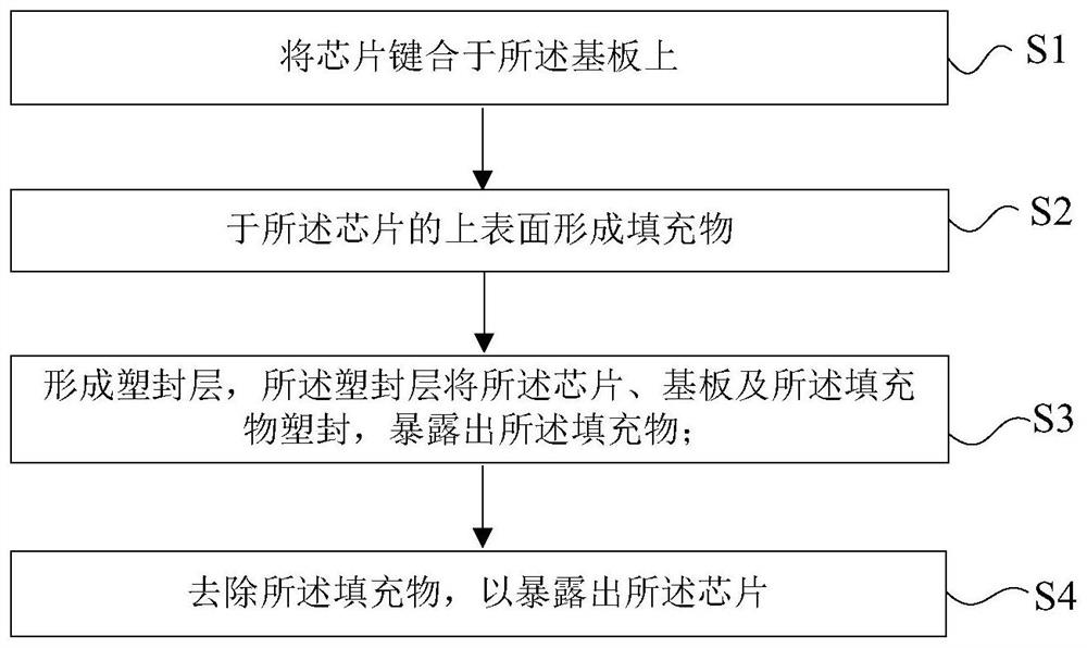
[0026] see figure 1 As shown, the present invention provides a method for preparing an encapsulation structure, comprising the steps of:

[0027] S1: bonding the chip on the substrate;

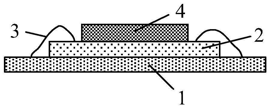
[0028] S2: forming a filler on the upper surface of the chip;

[0029] S3: forming a plastic sealing layer, the plastic sealing layer plastic sealing the chip, the substrate and the filler, exposing the filler;

[0030] S4: removing the filler to expose the chip.

[0031] The present invention is aimed at the surface exposed die (chip) packaging process, chooses to use the filler, and then takes it out after plastic sealing, avoiding the use of special-shaped molds, the size of the filler can be adjusted arbitrarily, the cost is low, and the process is simple; at the same time, the filler of the present invention The demoulding is clean, and there will be no filler residue on the surface of the chip.

Embodiment 2

[0033] Please combine figure 1 refer to Figures 2 to 7 , this embodiment also provides a method for preparing a packaging structure. The specific structure in this embodiment is roughly the same as that of the method for preparing the packaging structure in Embodiment 1. The difference between the two is that the packaging in this embodiment Compared with the method for preparing the packaging structure in Embodiment 1, the method for preparing the structure includes more and more detailed process steps.

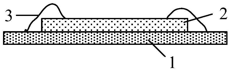
[0034] In step S1, the substrate 1 may include but not limited to PCB (Printed Circuit Board, printed circuit board).

[0035] Specifically, the chip 2 may be any chip with a device structure formed therein. More specifically, the device structure may be formed on the front side of the chip 2 .

[0036] In step S1 , the chip 2 may be mounted on the substrate 1 upright, that is, the chip 2 is bonded on the substrate 1 with its front facing up.

[0037] Such as figure 2...


PUM


Abstract

The invention provides a packaging structure and a preparation method thereof. The preparation method comprises the following steps: bonding a chip on a substrate; forming a filler on the upper surface of the chip; forming a plastic package layer to carry out plastic package on the chip, the substrate and the filler through the plastic package layer, and exposing the filler; and removing the filler so as to expose the chip. According to the surface die-exposed packaging technology, the mode of using the filler and taking out the filler after plastic packaging is selected, use of a special-shaped mold is avoided, the size of the filler can be adjusted at will, cost is low, and the technology is simple; meanwhile, the filler is demoulded cleanly, and no filler is left on the surface of the chip.

Description

technical field [0001] The invention relates to the technical field of semiconductor packaging, in particular to a packaging structure and a preparation method thereof. Background technique [0002] The traditional surface exposed die (chip) packaging process is realized by means of special-shaped molds, laser slotting, and direct exposed die. However, the price of special-shaped molds is very expensive, and laser grooving will cause chip damage. Direct exposure of die is only suitable for flip-chip chips. Many limitations lead to the defects of difficult die packaging, high cost and low yield. Contents of the invention [0003] In order to achieve the above purpose and other related purposes, the present invention provides a method for preparing a packaging structure, including: [0004] Bond the chip on the substrate; [0005] forming a filler on the upper surface of the chip; [0006] forming a plastic sealing layer, the plastic sealing layer plastic sealing the chi...

Claims


Application Information

Patent Timeline
Patent Type & Authority Applications(China)
IPC IPC(8): H01L21/56H01L23/31
CPCH01L21/56H01L23/3185H01L23/3171
Inventor 吴江唐伟炜丁海春周仪张竞扬徐明广龚凯柯军松徐晓枫李广钦熊进宇刘阳吴庆华孙涛戴文兵张世铭叶沛
Owner 合肥速芯微电子有限责任公司
Why Eureka
Try Eureka