
Driving circuit and display panel

A technology for driving circuits and display panels, applied to static indicators, instruments, etc.

Active Publication Date: 2021-09-07
WUHAN CHINA STAR OPTOELECTRONICS SEMICON DISPLAY TECH CO LTD
View PDF16 Cites 1 Cited by
  • Summary
  • Abstract
  • Description
  • Claims
  • Application Information

AI Technical Summary

Problems solved by technology

[0003] Embodiments of the present invention provide a driving circuit and a display panel, which can reduce the problem that the luminance of a light-emitting device varies greatly with time within one frame due to potential changes at the connection nodes connected to transistors

Method used


Image

  • Driving circuit and display panel
  • Driving circuit and display panel
  • Driving circuit and display panel

Examples


Embodiment Construction

[0022] Next, the technical solutions in the embodiments of the present invention will be apparent from the embodiment of the present invention, and it is clearly described, and it is understood that the described embodiments are merely embodiments of the present invention, not all of the embodiments. Based on the embodiments of the present invention, those skilled in the art are in the range of the present invention in the scope of the present invention without all other embodiments obtained without creative labor. In addition, it should be understood that the specific embodiments described herein are intended to illustrate and explain the invention and is not intended to limit the invention. In the present invention, when not explained, the orientation words used, such as "upper" and "under" generally refer to the upper and lower and bottoms of the apparatus in actual use or working state, specifically in the drawing direction in the drawings. And "inner" and "outside" are for th...


PUM


Abstract

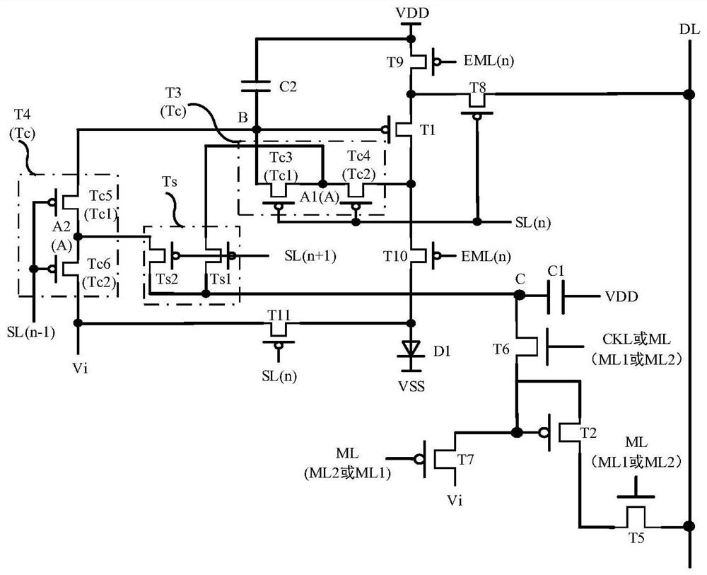
The invention provides a driving circuit and a display panel. The driving circuit comprises a driving module and an additional module, the driving module comprises a first transistor electrically connected with the first signal line and a connecting transistor connected with a grid electrode of the first transistor, and the connecting transistor is provided with a connecting node; the additional module comprises a second transistor having the same threshold voltage as the first transistor, and the second transistor is connected between the connection node and the first signal line, so that the voltage between the connection node and the grid electrode of the first transistor is reduced through the second transistor and the first signal line, and the potential variation at the connection node is reduced within a frame time. Therefore, the problem that the light-emitting brightness of the light-emitting device changes greatly along with time within one frame of time is solved, and the problem that the display panel is prone to flicker when low-frequency driving is achieved is solved.

Description

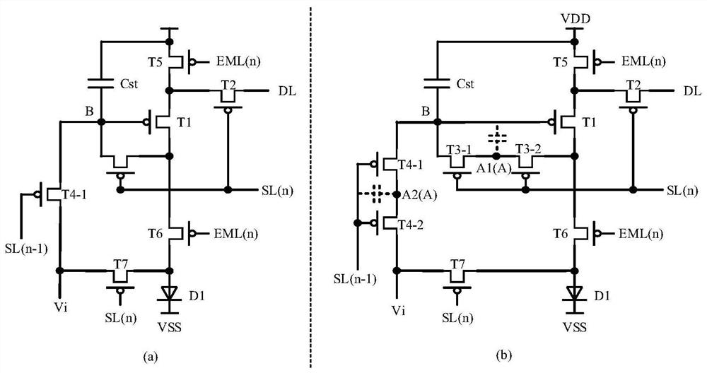
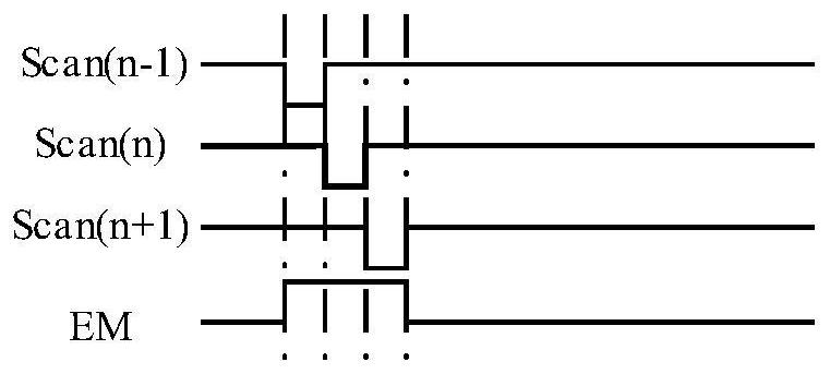
Technical field [0001] TECHNICAL FIELD The present invention relates in particular to a driving circuit and a display panel. Background technique [0002] Conventional display panel such as a multi-use Figure 1A 7T1C pixel driving circuit shown in (a) as complex Figure 1B To drive the drive timing shown in FIG device emits light, but in the emission phase, there is a leakage current of the transistor T3 and the transistor T4, the gate voltage of the transistor T1 impact (i.e., potential at the point B) of the stability, affecting the stability of the luminance of the light emitting device , resulting in the display screen of the display panel brightness decrease with time. Thus to reduce leakage current effects on the display screen, the transistors T3 and T4 dual-gate design, such as Figure 1A (B) shown in. But in the actual panel production process, it will inevitably have a parasitic capacitance, resulting in a potential difference between the point A1 and T3-1 T3-2, the poten...

Claims


Application Information

Patent Timeline
IPC IPC(8): G09G3/32G09G3/3208
CPCG09G3/32G09G3/3208G09G2320/0214G09G2300/0819G09G2300/0861G09G2300/0852G09G3/3233G09G2320/0219G09G2340/0435G09G2310/08G09G2320/0233
Inventor 曾勉孙亮
Owner WUHAN CHINA STAR OPTOELECTRONICS SEMICON DISPLAY TECH CO LTD
Learn More