Silicon carbide flaw detection equipment

A defect detection, silicon carbide technology, applied in optical testing of defects/defects, measuring devices, material analysis by optical means, etc., can solve the problems of laborious and inaccurate detection, and achieve the effect of convenient detection and accurate detection results.

Pending Publication Date: 2021-09-17
上海谦视智能科技有限公司
View PDF0 Cites 0 Cited by
  • Summary
  • Abstract
  • Description
  • Claims
  • Application Information

AI Technical Summary

Problems solved by technology

[0003] To this end, the embodiment of the present invention provides a silicon carbide defect detection device to solve the problem in the prior art that the detection is relatively laborious and not accurate enough due to direct observation of whether the silicon carbide substrate has defects with the naked eye

Method used


Image

  • Silicon carbide flaw detection equipment
  • Silicon carbide flaw detection equipment
  • Silicon carbide flaw detection equipment

Examples


Embodiment 1

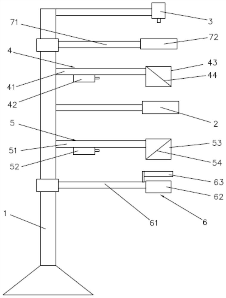
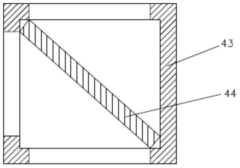
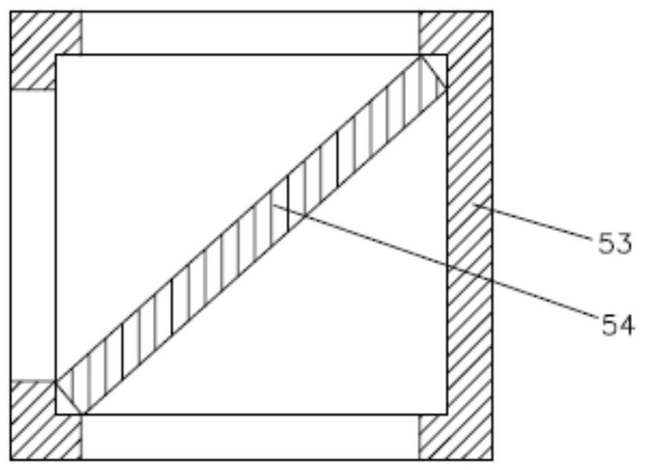
[0023] A silicon carbide defect detection device, such as Figure 1-3 As shown, it includes a support frame 1, a support rod is fixedly connected to the upper end of the support frame 1, and an imaging device is fixedly connected to the support rod. The imaging device can be a camera, or a combination of a camera and some lenses. The imaging device used in the present invention for camera 3. In addition, a bearing rod is fixedly connected to the middle part of the support frame 1, and a loading platform 2 is fixedly connected to the loading rod. The loading platform 2 is made of a transparent material, and the camera 3 is located directly above the loading platform 2. A through hole is provided, and the camera 3 can be used to photograph the situation of the stage 2 coming out. The position where the support frame 1 is located between the camera 3 and the stage 2 is provided with a first light source 4 directed toward the stage 2, and the position where the support frame 1 is...

Embodiment 2

[0034] A silicon carbide defect detection device, the difference from Embodiment 1 is, such as Figure 5 As shown, the device is not provided with a separate polarized light source, and a second camera 8 is provided at the position where the support frame 1 is located below the stage 2, and the second camera 8 is fixedly connected to the support frame 1 through a connecting rod. The illuminating end of the second camera 8 faces the central position of the stage 2, and the second camera 8 is below the transmitted light source 5; in addition, a third polarizer 9 is arranged between the transmitted light source 5 and the stage 2, and the third polarizer 9 is connected to the support frame 1 through a fixed rod, and the fixed rod can move around the support frame 1 to make it move to other positions. In this way, when detecting the lower surface of the silicon carbide substrate sheet, the reflected light after the transmission light source 5 is irradiated to the back surface of th...


PUM


Abstract

The embodiment of the invention discloses silicon carbide flaw detection equipment, and belongs to the technical field of semiconductor detection. According to the technical scheme, the equipment comprises a supporting frame, an objective table and an imaging device are arranged on the supporting frame, the imaging device is located above the objective table, and a through hole is formed in the objective table; a first light source irradiating to the objective table is arranged at the position, between the imaging device and the objective table, of the supporting frame, and a transmission light source irradiating to the objective table is arranged at the position, below the objective table, of the supporting frame; a polarized light source irradiating the objective table is further arranged at the position, below the transmission light source, of the supporting frame; a polarization tester is arranged at a position, below the imaging device, of the support frame; and the polarization tester can rotate and is separated from the right lower part of the imaging device. The invention can solve the problems that in the prior art, due to the fact that whether flaws exist on a silicon carbide substrate or not is directly observed with naked eyes, detection is relatively strenuous and not accurate enough.

Description

technical field [0001] Embodiments of the present invention relate to the technical field of semiconductor detection, and in particular to a silicon carbide defect detection device. Background technique [0002] The silicon carbide substrate is a translucent wafer. At present, the crystal material of the silicon carbide substrate produces various defects during the growth process, including defects in the substrate such as micropipes, wrapping, or defects on the surface of the substrate such as scratches. , collapse and so on. Therefore, different methods are used in the industry to check and detect these defects. The current detection method is generally through manual observation, and directly observes whether the silicon carbide substrate has defects with the naked eye. This is relatively laborious and the detection is not accurate enough. Contents of the invention [0003] Therefore, an embodiment of the present invention provides a silicon carbide defect detection de...

Claims


Application Information

Patent Timeline
Patent Type & Authority Applications(China)
IPC IPC(8): G01N21/95
CPCG01N21/8806G01N21/9501G01N21/9505G01N2021/8841G01N2021/8848
Inventor 黄英俊
Owner 上海谦视智能科技有限公司
Why Eureka
Try Eureka