Chip and pin outgoing line design method thereof

A design method and chip technology, applied in computer-aided design, calculation, special data processing applications, etc., can solve problems such as unprovided, chip pin outlet design quality is uneven, etc., to achieve refined design and ensure the quality of outlet design Effect

Active Publication Date: 2021-09-24
SUZHOU LANGCHAO INTELLIGENT TECH CO LTD
View PDF3 Cites 1 Cited by
  • Summary
  • Abstract
  • Description
  • Claims
  • Application Information

AI Technical Summary

Problems solved by technology

However, the prior art does not provide a unified chip pin-out design for BGA-packaged chips, which...

Method used


Image

  • Chip and pin outgoing line design method thereof
  • Chip and pin outgoing line design method thereof
  • Chip and pin outgoing line design method thereof

Examples


Embodiment Construction

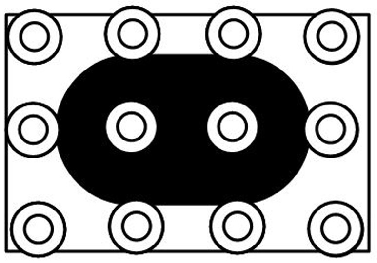
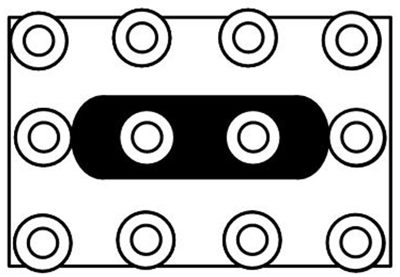
[0053] The core of the present invention is to provide a chip and its pin outlet design method, which provides a unified chip pin outlet design for BGA-packaged chips, and the design is relatively refined, thereby ensuring the chip pin outlet design quality.

[0054] In order to make the purpose, technical solutions and advantages of the embodiments of the present invention clearer, the technical solutions in the embodiments of the present invention will be clearly and completely described below in conjunction with the drawings in the embodiments of the present invention. Obviously, the described embodiments It is a part of embodiments of the present invention, but not all embodiments. Based on the embodiments of the present invention, all other embodiments obtained by persons of ordinary skill in the art without making creative efforts belong to the protection scope of the present invention.

[0055] Please refer to figure 1 , figure 1 It is a flow chart of a chip pin outle...


PUM


Abstract

The invention discloses a chip and a pin outgoing line design method thereof, which are applied to a BGA packaged chip. The method comprises the following steps of determining the number of layers of circuit boards required by the pin outgoing lines of the chip according to the pin position information and the pin definition information of the chip; distributing the respective outgoing lines layers on the circuit boards for the pins of the chip; and according to the pin density of the chip and the width requirement of the transmission lines, determining the specification of a via hole for leading out the pins of the chip to the corresponding outgoing line layer on the circuit board so as to carry out the corresponding wire outlet design based on the via hole. Therefore, the invention provides a unified chip pin outgoing line design aiming at the BGA packaged chip, and the design is more refined, so that the outgoing line design quality of the chip pin is ensured.

Description

technical field [0001] The invention relates to the field of high-speed and high-density chips, in particular to a chip and a pin outlet design method thereof. Background technique [0002] In recent years, servers and communication products continue to pursue high-density and miniaturized designs, resulting in higher and higher requirements for chip density. With the development of high-speed transmission technology, most of the chip signals are designed as high-speed signals. At present, high-speed and high-density chips are all packaged in BGA (Ball Grid Array, ball grid array), and the most critical link is the pin (pin) outlet design of the chip. However, the prior art does not provide a uniform chip pin outlet design for BGA-packaged chips, and designers design according to their own experience, resulting in uneven chip pin outlet design quality. [0003] Therefore, how to provide a solution to the above technical problems is a problem that those skilled in the art ne...

Claims


Application Information

Patent Timeline
IPC IPC(8): G06F30/343
CPCG06F30/343G06F30/392G06F30/396G06F30/394G06F2113/18G06F2115/12G01N2035/0436H05K2201/09227
Inventor 梁磊秦清松
Owner SUZHOU LANGCHAO INTELLIGENT TECH CO LTD
Why Eureka
Try Eureka