Supercharge Your Innovation With Domain-Expert AI Agents!

Display device and spliced display module

A display device and display module technology, applied in the direction of identification devices, instruments, etc., can solve the problems of image discontinuity, low resolution, and the width of the surrounding area cannot be reduced, and achieve the effect of reducing the impact of visual discontinuity and reducing the width

Active Publication Date: 2021-09-28
AU OPTRONICS CORP
View PDF16 Cites 0 Cited by
  • Summary
  • Abstract
  • Description
  • Claims
  • Application Information

AI Technical Summary

Problems solved by technology

However, due to the characteristics of ACF, the conductive particles in ACF are arranged in a two-dimensional manner. In order to maintain the quality of the signal, the contact area needs to maintain a sufficient contact area. This is also the main reason why the width of the peripheral area cannot be reduced.
[0004] In addition to affecting the utilization of the substrate, the width of the peripheral area, in many current large-scale occasions, such as concerts, will form a large-scale display by splicing multiple displays Display screen, when the width of the peripheral area is too large, it will visually cause discontinuous images and low resolution

Method used


Image

  • Display device and spliced display module
  • Display device and spliced display module
  • Display device and spliced display module

Examples


Embodiment Construction

[0065] The technical solutions of the present invention will be described in detail below with reference to the accompanying drawings and specific examples, in detail to the objects, schemes and efficacy of the present invention, but are not limited to the scope of claims appended claims.

[0066] It should be understood that when the element is called "connection" or "setting" at another element, it can represent the element to be directly positioned, or the intermediate element can also be contacted, and the component is connected to another element. Conversely, when the element is referred to as "directly on another element" or "directly connected to another element", it is understood that there is no intermediate element at this time.

[0067] In addition, the term "first", "second", "third" These terms are only used to separate one element, component, region, or portion with another element, component, region, layer or part, rather than Its necessarily order. Further, relativ...


PUM

PropertyMeasurementUnit
Widthaaaaaaaaaa

Abstract

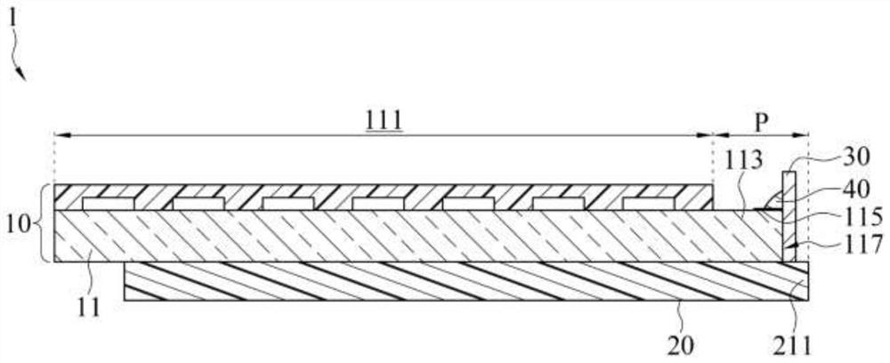
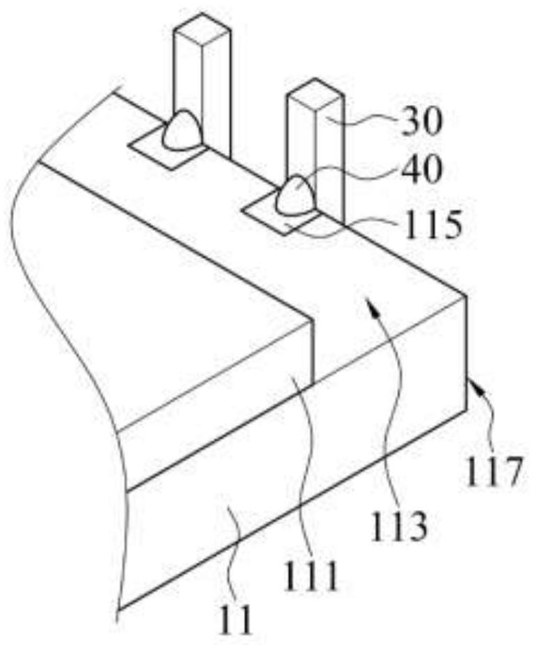
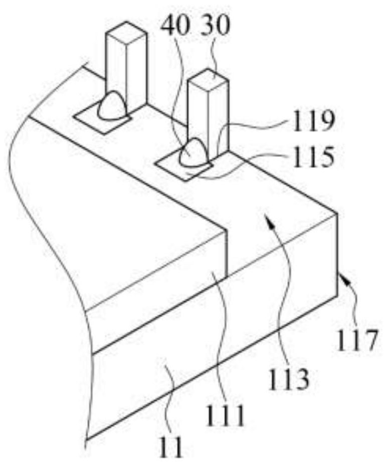
A display device includes a display unit, a circuit board, a plurality of conductive probes, and a plurality of conductive glues. The display unit includes a display substrate. The front of the display substrate includes a display area and a circuit area. The circuit area is located on the periphery of the display substrate, and the circuit area has a plurality of connection pads. The circuit board is located on the back of the display substrate, and the connection area of the circuit board does not overlap with the display substrate. Each conductive probe is arranged on the connection area of the circuit board, is in contact with the side edge of the display substrate, and extends beyond the top of the display substrate. Each conductive probe corresponds to one of the connection pads. Each conductive glue connects the conductive probe and the corresponding connection pad. The conductive probes and conductive particles are three-dimensionally distributed conductive glue, which can reduce the width of the peripheral area of the display, and expand the proportion of the display area in the same display substrate size.

Description

Technical field [0001] The present invention relates to the field of displays, in particular to a display device and a splicing display module. Background technique [0002] On the production of the display, the display substrate is pursuing the maximum display area ratio as the target, however, the current display device is a circuit area of ​​the display substrate, and a circuit board located below the display substrate, and electricity by bending the soft circuit board Sexual connection. Since the bending soft circuit board is to retain a certain space, the width of the surrounding area of ​​the display is currently the width of the display substrate in the display area, the drive circuit board and the display substrate are not overlapped. As well as the total width of the soft circuit board bent out of 1.8 to 8 mm, depending on the size and setting of the actual panel. [0003] Further, since the circuit board and the display substrate are connected by a soft circuit board, i...

Claims


Application Information

Patent Timeline
IPC IPC(8): G09F9/302
CPCG09F9/3026
Inventor 何俊樟郑文琳
Owner AU OPTRONICS CORP
Features
  • R&D
  • Intellectual Property
  • Life Sciences
  • Materials
  • Tech Scout
  • Unparalleled Data Quality
  • Higher Quality Content
  • 60% Fewer Hallucinations
Learn More