Micro-connection and separation device for sealing, testing and processing PLC type optical chip and use method of micro-connection and separation device

A separation device and micro-connection technology, used in electrical components, semiconductor/solid-state device manufacturing, circuits, etc., to solve problems such as excessive force and damage

Active Publication Date: 2021-10-12
HARBIN YULONG AUTOMATION
View PDF20 Cites 0 Cited by
  • Summary
  • Abstract
  • Description
  • Claims
  • Application Information

AI Technical Summary

Problems solved by technology

[0004] The purpose of the present invention is to provide a PLC-type optical chip packaging and testing micro-connection separation device and its use method, to solve the problem of excessive force when the hand-held blade cuts off the upper and lower shell adhesion parts when cutting proposed in the above background technology. Large problem of damage to pins

Method used


Image

  • Micro-connection and separation device for sealing, testing and processing PLC type optical chip and use method of micro-connection and separation device
  • Micro-connection and separation device for sealing, testing and processing PLC type optical chip and use method of micro-connection and separation device
  • Micro-connection and separation device for sealing, testing and processing PLC type optical chip and use method of micro-connection and separation device

Examples


Embodiment Construction

[0029] The following will clearly and completely describe the technical solutions in the embodiments of the present invention with reference to the accompanying drawings in the embodiments of the present invention. Obviously, the described embodiments are only some, not all, embodiments of the present invention. Based on the embodiments of the present invention, all other embodiments obtained by persons of ordinary skill in the art without making creative efforts belong to the protection scope of the present invention.

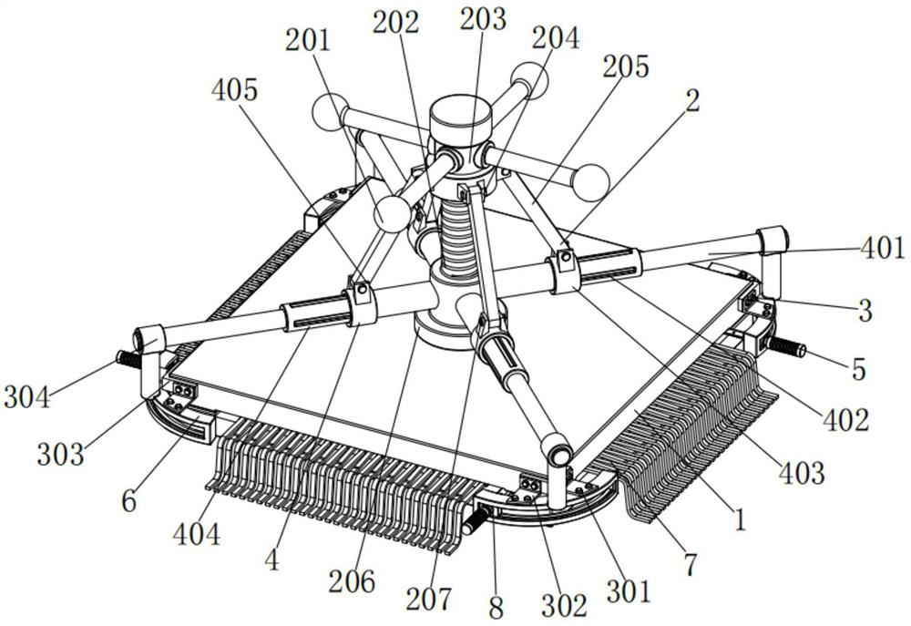
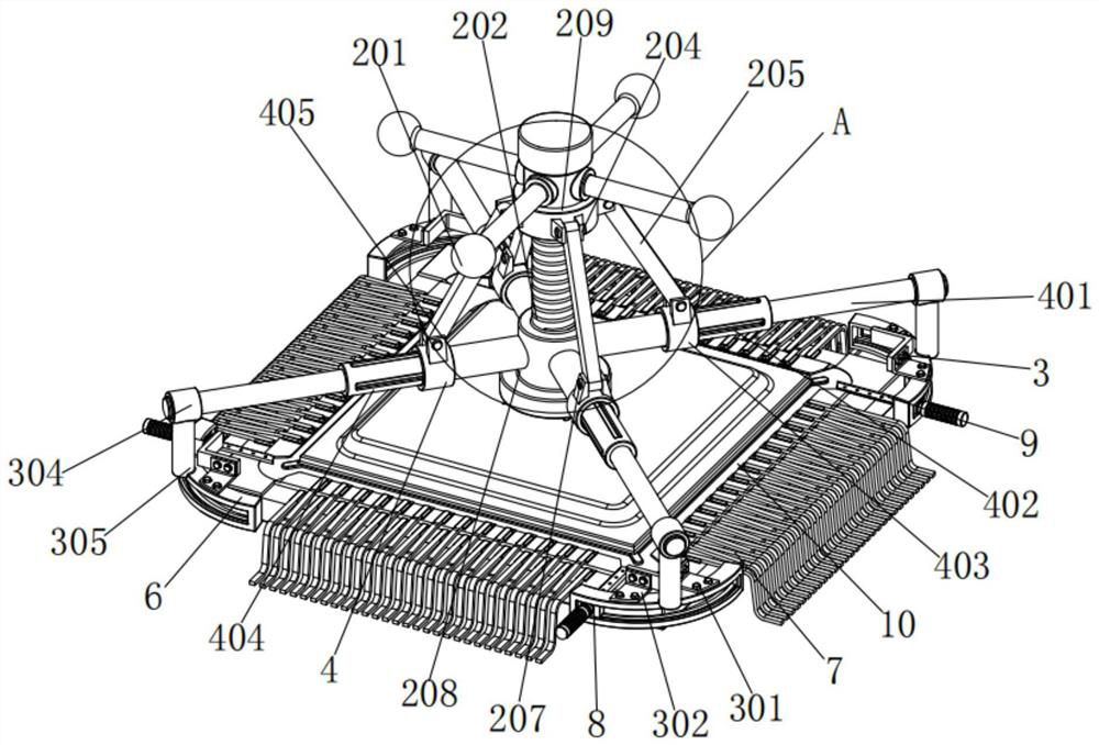
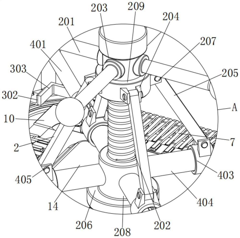
[0030] see Figure 1-6, the present invention provides a technical solution: a PLC type optical chip packaging and testing micro-connection separation device, comprising an upper housing 1 and a lower housing 10, the lower end of the upper housing 1 is bonded with the lower housing 10, the upper The inner side of housing 1 and lower housing 10 is equipped with chip 14, and chip 14 is PLC type optical chip, and the outer wall of chip 14 is connected with a plur...


PUM


Abstract

The invention discloses a micro-connection and separation device for sealing, testing and processing a PLC type optical chip and a use method of the micro-connection and separation device, and relates to the technical field of chip sealing and testing. The micro connection and separation device for sealing, testing and processing the PLC type optical chip comprises an upper shell and a lower shell, the lower end of the upper shell is bonded with the lower shell, chips are installed at the inner sides of the upper shell and the lower shell, and a transmission mechanism is installed at the tail end of the outer side of the driving mechanism. According to the micro-connection separating device for sealing, testing and processing the PLC type optical chip, through the cooperation of a blade, a base, a gasket, a blade, a main cutting edge, the upper shell, the lower shell, a frame and a sliding block, the upper shell and the lower shell can be separated by pressing the upper portion of the base with a hand, the chip can be conveniently overhauled or replaced and repackaged, and the sliding block is limited by the angle of the frame in the sliding process, so that the problem that when an existing handheld blade cuts the adhesion portion of the upper shell and the lower shell, a pin is damaged due to too large force is solved.

Description

technical field [0001] The invention relates to the technical field of chip packaging and testing, in particular to a PLC-type optical chip packaging and testing micro-connection separation device and a use method. Background technique [0002] Chip packaging and testing refers to the process of processing wafers that pass the test according to the product model and its functional requirements, and then obtaining independent chips. Chip packaging and testing is the basis of modern technology. Many devices need to use chips, such as Mobile phones, computers, etc., have the current high-tech equipment because of the composition of these chips. After the packaging and testing is completed, usually the upper and lower shells can be installed on the outside of the chip by bonding together, and the chip is repaired or replaced. , it is usually necessary to cut off the upper and lower shells to separate them, although the existing technology can cut off the adhesion of the upper an...

Claims


Application Information

Patent Timeline
Patent Type & Authority Applications(China)
IPC IPC(8): H01L21/67H01L21/687
CPCH01L21/67092H01L21/67144H01L21/67242H01L21/68721
Inventor 刘志超杨晓伟
Owner HARBIN YULONG AUTOMATION
Why Eureka
Try Eureka