Broadband power combining device using antipodal finline structure

a technology of antipodal fins and combining devices, which is applied in coupling devices, waveguides, electrical apparatus, etc., can solve the problems of short life time, poor linearity, and high cost, and achieve the effect of minimizing both thermal resistance from chip to carrier and rf parasitic noise, reducing system complexity, and maximizing combining efficiency

Active Publication Date: 2007-05-08
CW ACQUISITION
View PDF17 Cites 305 Cited by
  • Summary
  • Abstract
  • Description
  • Claims
  • Application Information

AI Technical Summary

Benefits of technology

[0016]The wedge shaped carriers in the device provide a DC bias path and good thermal management. Slots or holes are machined in the middle of the metal carrier for DC lines. When the trays are stacked together, DC bias lines will be connected to inside active elements through those slots or holes. Active elements are eutectically attached to the center of the metal carrier. It will minimize the thermal resistance from active element to the outside heat sink.
[0017]The antipodal finline is disposed on a soft board substrate material and can be manufactured by a conventional PCB process. The antipodal finline has a tapered conductor on the top side of the substrate and a tapered conductor on the back side. The top side conductor tapers to about half of the board width, then tapers to a narrow strip, which becomes a microstrip line. The back side conductor tapers to about half of the board width, then tapers to the full board width which will become the ground for the top side microstrip line. Since the tolerance for back side to top side alignment is not tight and all the dimensions are large enough, it is much easier to manufacture as compared with circuits using a slotline to microstrip balun and still offers good compatibility with COTS MMIC's.
[0019]By using antipodal finlines, the invention achieves the broadest bandwidth that has ever been practically achieved by a spatial power combiner. Moreover, the antipodal finline design makes it possible to fabricate the circuit with a PCB process. It simplifies the assembly process and dramatically reduces the cost for manufacturing.
[0021]In the presently claimed invention, individually packaged MMICs are used in the combining device. The packages are hermetically sealed. Since all the other elements are passive, the whole structure is considered hermetically sealed. This will significantly reduce the complexity of the system and make it accessible for easy repair.
[0022]The packages of the invention are also surface mountable and have a metal base which is soldered to the metal tray. RF input / output ports are soldered to the microstrip line of the antipodal finline structure. The soldering connections will minimize both thermal resistance from chip to carrier and RF parasitic noise.
[0023]In another aspect of the invention, there is provided an innovative biasing scheme to maximize the combining efficiency for spatial waveguide power combining devices. Since MMIC's are used as active elements, the maximum combining efficiency will be achieved when all the MMIC's have uniform performance. Loss can be caused by amplitude and phase variation among the elements. The current semiconductor integrated circuits still have considerable variations from die to die. In most of the amplifier MMIC's, the semiconductor devices are GaAs HEMTs (high electron mobility transistor) which use gate voltage to control the output current. To insure each element is putting out the same amount of power, a feedback circuit is used to sense the drain current and lock it to a fixed value by adjusting gate voltage. Since the load for each active element is the same, for a fixed drain current, the output power will be the same too. This scheme helps to improve the power combining efficiency for spatial waveguide power combining devices.

Problems solved by technology

However, several drawbacks are associated with TWTAs, including short life-time, poor linearity, high cost, large size and weight, and the requirement of a high voltage drive, imposing high voltage risks.
However, currently, the best available broadband solid state amplifiers can only offer output power in a watt range covering about 2 to 20 GHz frequency band.
A typical corporate combining technique can lead to very high combining loss when integrating a large amount of amplifiers.
Since the dominant mode inside the rectangular waveguide is TE10 mode, the combiners also have a dispersion problem over the whole waveguide band.
However, as in U.S. Pat. No. 5,736,908 and other prior art, the bandwidth of the system is limited by the rectangular waveguide used.
This arrangement suffers from serious heat dissipation issues, as it is difficult to remove heat effectively from the power devices to an outside heat sink since the heat spreads to the slotline card first, then conducts to the waveguide through the sliding contacts between the slotline card and the waveguide.
The heat increases the operation temperature and decreases the lifetime of the amplifiers dramatically.
Moreover, it is difficult to connect outside DC bias into the active devices on the slotline cards, and to access the slotline cards generally, as these are disposed inside an enclosed waveguide structure.
Even though a metal tray is added underneath the slotline card, the thermal resistance caused by many layers of material and junctions remains problematic when high power devices are used.
Since bonding wires are used to connect from slotline to MMIC which is not on the same layer, the parasitic effect will deteriorate the performance at higher frequency band.
Further, assembly complications and costs are high.
The accurate back side-to-top side alignment requirement significantly complicates the manufacturing process.
This increases costs dramatically, and since the ceramics are fragile, it raises significant reliability issues.

Method used


Image

  • Broadband power combining device using antipodal finline structure
  • Broadband power combining device using antipodal finline structure
  • Broadband power combining device using antipodal finline structure

Examples


Embodiment Construction

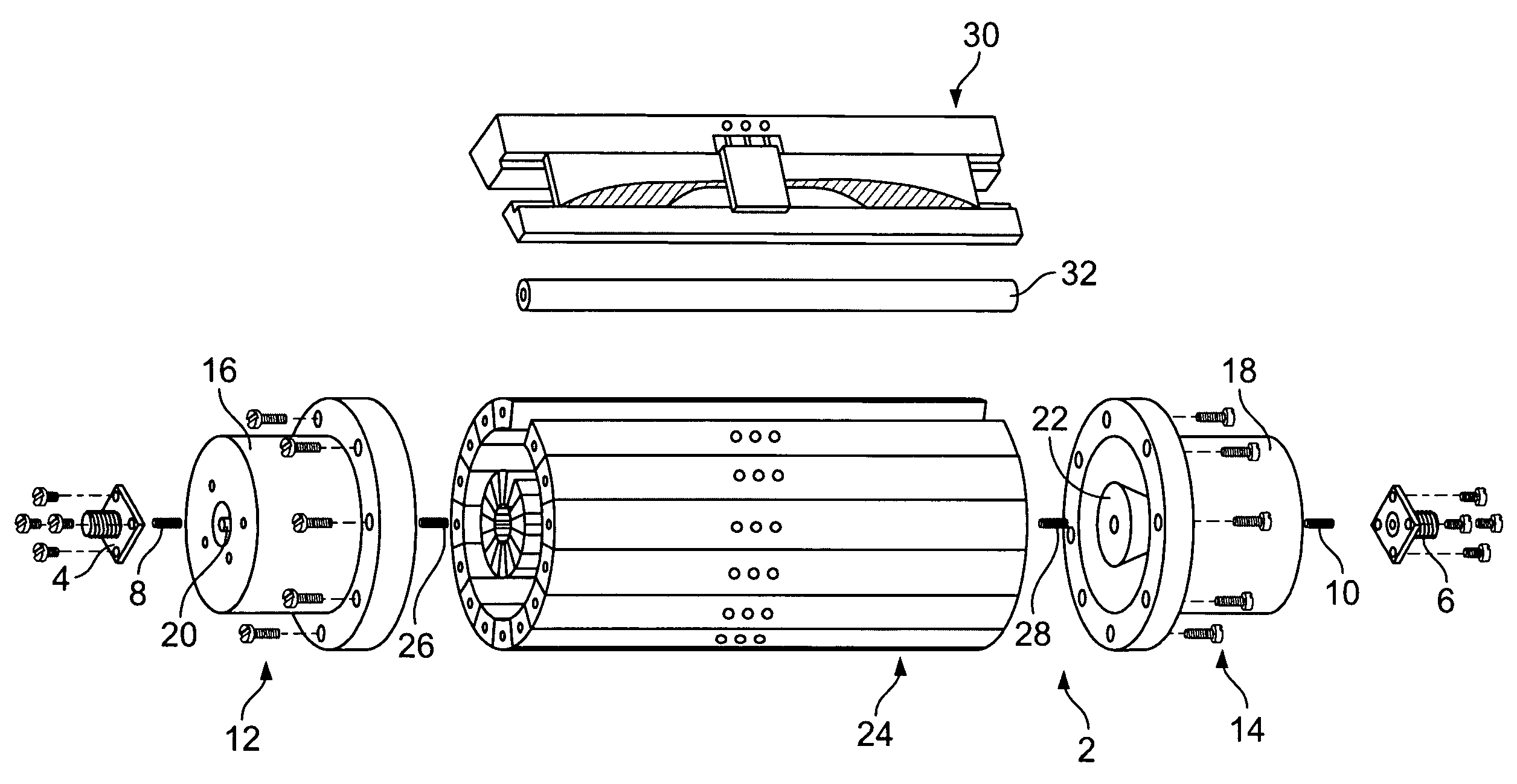
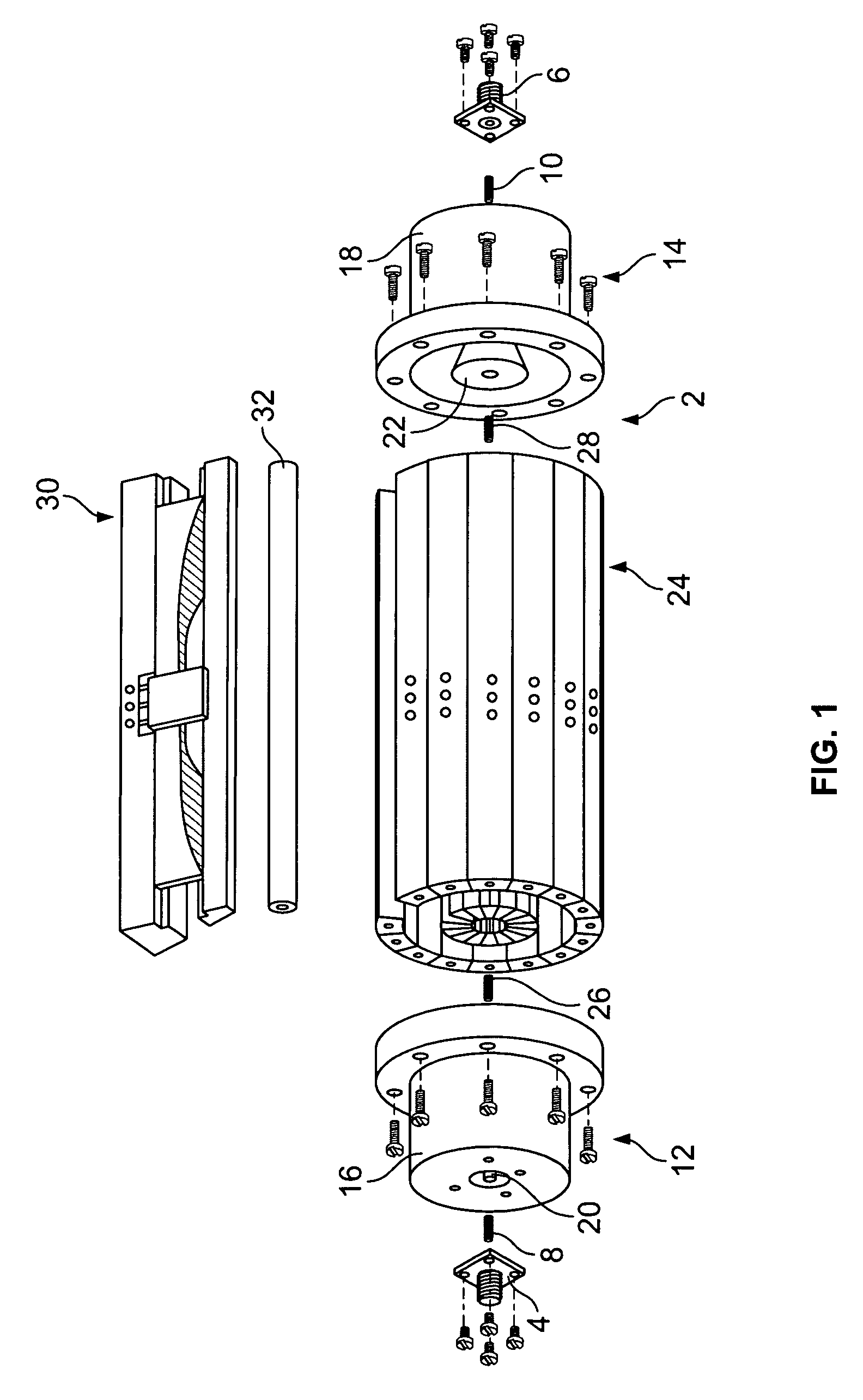
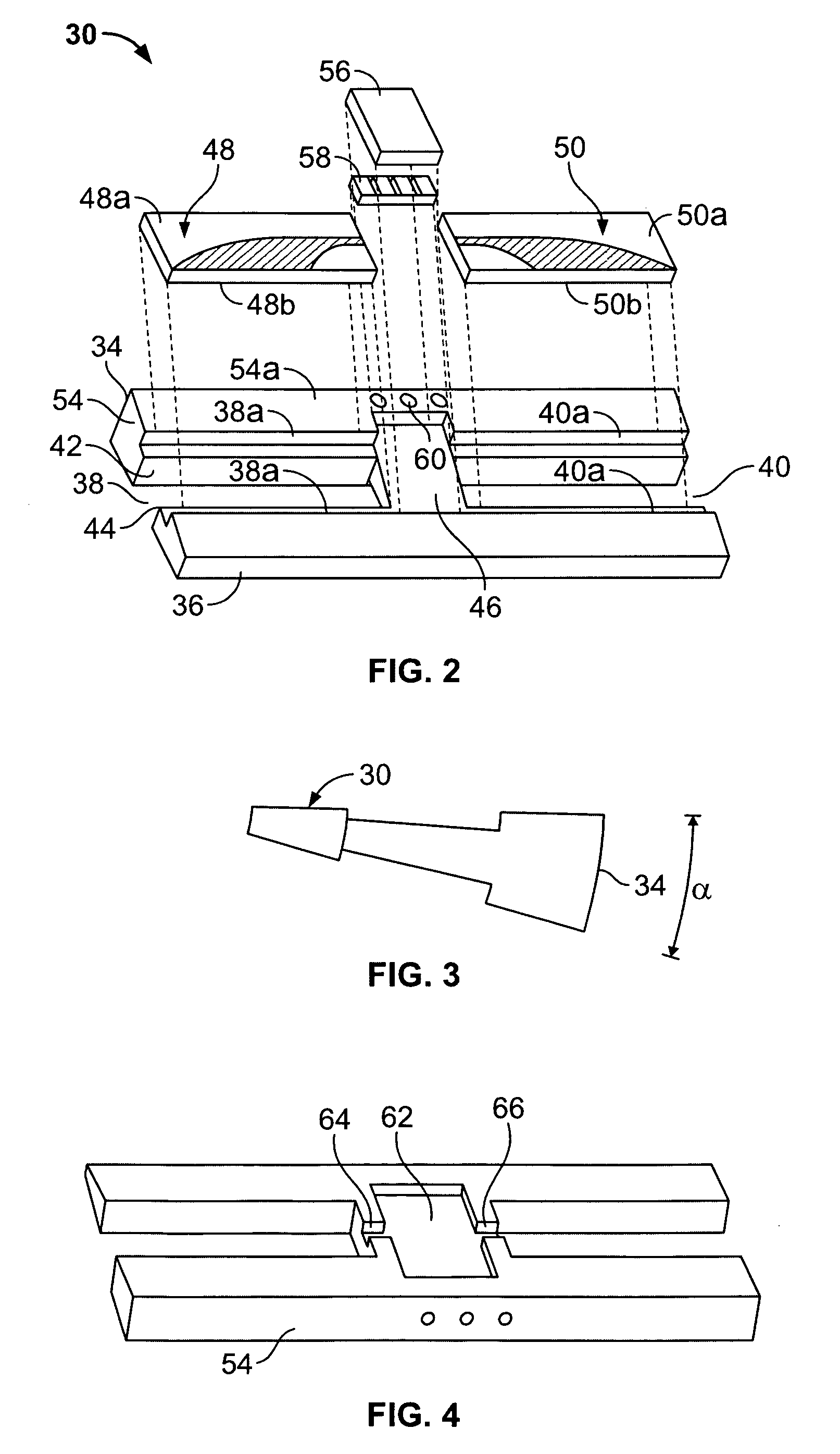
[0045]In accordance with the invention, a broadband spatial power combining device using longitudinally parallel, stacked wedge shaped trays is provided. Antipodal finline structures are mounted on each tray. When the trays are stacked together to form a coaxial waveguide, the antipodal finline structures are disposed into the waveguide and form a dividing array at the input and a combining array at the output. With the use of antipodal finline arrays inside the coaxial waveguide for power dividing and combining, a broadband frequency response covering the range of about 2 to 20 GHz is realized. The antipodal finline structure is easy to manufacture using conventional printed circuit board (PCB) processes. It also enables easy integration with COTS (commercial off-the-shelf) MMICs. Further, the division of a coaxial waveguide into wedge-shaped trays enables simplified DC biasing and provides good thermal management.

[0046]As illustrated in FIG. 1, in the spatial power combining devic...


PUM


Abstract

A broadband power combining device includes an input port, an input waveguide section, a center waveguide section formed by stacked wedge-shaped trays, an output waveguide section, and an output port. Each tray is formed of a wedge-shaped metal carrier, an input antipodal finline structure, one or more active elements, an output antipodal finline structure, and attendant biasing circuitry. The wedge-shaped metal carriers have a predetermined wedge angle and predetermined cavities. The inside and outside surfaces of the metal carriers and surfaces of the cavity all have cylindrical curvatures. When the trays are assembled together, a cylinder is formed defining a coaxial waveguide opening inside. The antipodal finline structures form input and output arrays. An incident EM wave is passed through the input port and the input waveguide section, distributed by the input antipodal finline array to the active elements, combined again by the output antipodal finlines array, then passed to the output waveguide section and output port. A hermetic sealing scheme, a scheme for improving the power combining efficiency and thermal management scheme are also disclosed. The broadband power combining device operates with multi-octave bandwidth and is easy to manufacture, well-managed thermally, and highly efficient in power combining.

Description

BACKGROUND OF THE INVENTION[0001]1. Field of the Invention[0002]The invention relates to a device for spatially dividing and combining power of an EM wave using a plurality of longitudinally parallel trays. More particularly, the invention relates to a device for dividing and combining the EM wave by antipodal finline arrays provided within a coaxial waveguide cavity.[0003]2. Description of the Related Art[0004]The traveling wave tube amplifier (TWTA) has become a key element in broadband microwave power amplification for radar and satellite communication. One advantage of the TWTA is the very high output power it provides. However, several drawbacks are associated with TWTAs, including short life-time, poor linearity, high cost, large size and weight, and the requirement of a high voltage drive, imposing high voltage risks.[0005]Solid state amplifiers are superior to TWTAs in several aspects, such as cost, size, life-time and linearity. However, currently, the best available broadb...

Claims


Application Information

Patent Timeline
Patent Type & Authority Patents(United States)
IPC IPC(8): H01P5/12H01P3/08
CPCH01P5/12
Inventor JIA, PENGCHENG
Owner CW ACQUISITION
Why Eureka
Try Eureka