Pixel structure, manufacturing method of pixel structure and array substrate

A pixel structure and pixel technology, applied in nonlinear optics, instruments, optics, etc., can solve the problems of high power consumption of liquid crystal panels, achieve high contrast, increase viewing angle, and save costs.

Pending Publication Date: 2021-10-22
SHENZHEN LAIBAO HI TECH
View PDF0 Cites 1 Cited by
  • Summary
  • Abstract
  • Description
  • Claims
  • Application Information

AI Technical Summary

Problems solved by technology

[0004] The purpose of the embodiment of the present application is to provide a pixel structure to solve the problem of high power consumption of the liquid crystal panel in the existing AIFF MVA mode

Method used


Image

  • Pixel structure, manufacturing method of pixel structure and array substrate
  • Pixel structure, manufacturing method of pixel structure and array substrate
  • Pixel structure, manufacturing method of pixel structure and array substrate

Examples


Embodiment Construction

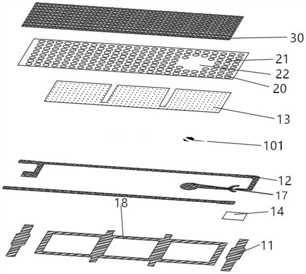
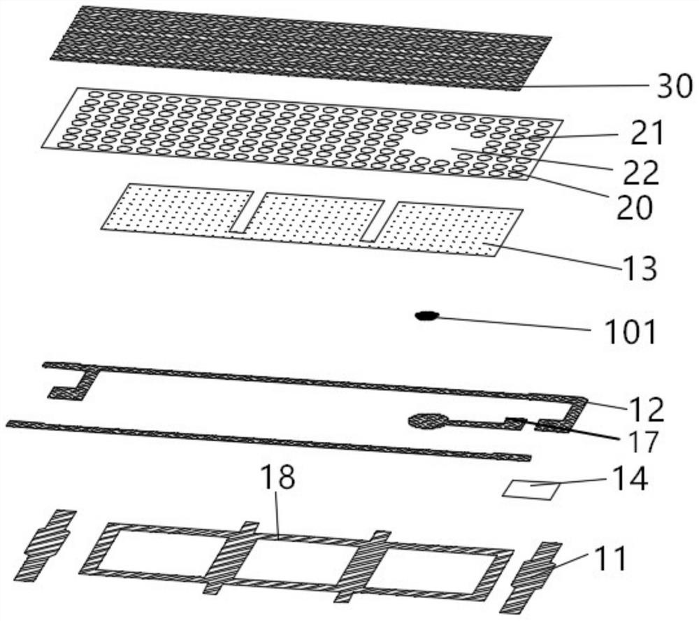
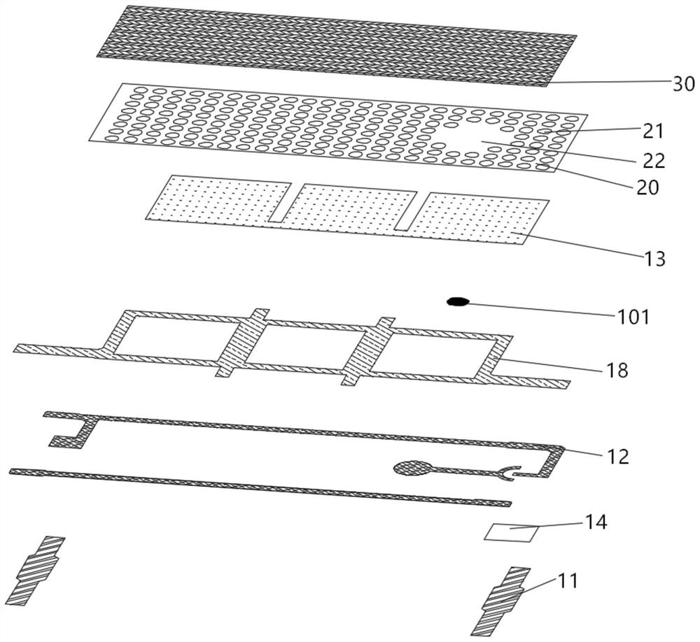
[0043] In order to make the technical problems, technical solutions and beneficial effects to be solved, the present application will be described in detail below with reference to the accompanying drawings and examples. It should be understood that the specific embodiments described herein are intended to explain the present application and is not intended to limit the present application.

[0044] It should be noted that when the element is referred to as "fixed to" or "set to" another element, it can be directly on the other element or indirectly on the other element. When a component is called "connected to" another element, it can be directly connected to another element or indirectly connected to the other element.

[0045] It is to be understood that the term "length", "width", "upper", "lower", "front", "post", "right", "vertical", "level", "top" , "Bottom", "inside", "outside", etc., the orientation of the orientation is based on the orientation or positional relationship...


PUM


Abstract

The invention belongs to the technical field of panel display, and particularly relates to a pixel structure, a manufacturing method of the pixel structure and an array substrate. A diffuse reflection structure and a mirror reflection structure are arranged on a reflection substrate layer, a reflection layer covers the diffuse reflection structure and the mirror reflection structure and presents shapes corresponding to the diffuse reflection structure and the mirror reflection structure, and when incident light irradiates the position, corresponding to the diffuse reflection structure, of the reflection layer, the reflection layer conducts diffuse reflection on the incident light; when incident light irradiates the position, corresponding to the specular reflection structure, of the reflection layer, the reflection layer conducts specular reflection on the incident light. Therefore, the functions of diffuse reflection and specular reflection of light are achieved, the display device with the structure has high reflectivity, diffuse reflection and specular reflection are beneficial for increasing the lateral visual angle, a backlight source structure does not need to be used, overall power consumption is reduced, cost is saved, and meanwhile the product further has the advantages of being wide in visual angle and high in contrast ratio.

Description

Technical field [0001] The present invention belongs to the field of flat panel display, and more particularly to a method of fabricating a pixel structure, a pixel structure, and an array substrate. Background technique [0002] Currently, the display mode of TFT-LCD (Thin Film Transistor Liquid Crystal Display) mainly has TN (Twisted Nematic, Twisted Numbers) Mode, VA (VerticalAlignment, Vertical Orientation) Mode, IPS (in-Plane-Switching) , planar direction switching) mode, ADS (AdvancedSuper dimension Switch, superb dimensional field switching) mode, MVA (Muti-domain vertical alignment, multi-domain vertical alignment) mode, and AIFF MVA (Amiplified Intrinsic Fringe field ControlledMuti-domain vertical alignment, reinforced liquid crystal Inner edge electric field effect multi-domain vertical orientation) mode. [0003] The AIFF MVA mode has a wide range of views, but the liquid crystal panel of existing App AIFF MVA mode is displayed to provide a light source, and the backli...

Claims


Application Information

Patent Timeline
Patent Type & Authority Applications(China)
IPC IPC(8): G02F1/1335G02F1/1368G02F1/1362
CPCG02F1/133553G02F1/1368G02F1/136277
Inventor 乔传兴蔡昌宇颜金成赵约瑟
Owner SHENZHEN LAIBAO HI TECH
Why Eureka
Try Eureka