Intelligent super-junction MOS device and manufacturing method thereof

A MOS device and intelligent technology, which is applied in semiconductor/solid-state device manufacturing, semiconductor devices, electrical components, etc., can solve the problems of low isolation voltage and no real isolation, and achieve high isolation voltage and smooth electric field distribution.

Inactive Publication Date: 2021-10-26
滁州华瑞微电子科技有限公司
View PDF0 Cites 2 Cited by
  • Summary
  • Abstract
  • Description
  • Claims
  • Application Information

AI Technical Summary

Problems solved by technology

[0004] Figure 11 and 12 For the super-junction MOS isolation design of the prior art, only the P-type doped region pillars and N-type doped region pillars are arranged in a simple criss-cross arrangement. This design can meet the die withstand voltage requirements, but the isolation between MOS The voltage is less than 10V, and the withstand voltage curve is almost a resistive curve. After analysis, in this design, the active area of ​​sampling MOS and starting MOS is connected to the active area of ​​the main MOS after the process of high-temperature annealing , therefore, there is no real isolation between MOS, so the isolation voltage is very low

Method used


Image

  • Intelligent super-junction MOS device and manufacturing method thereof
  • Intelligent super-junction MOS device and manufacturing method thereof
  • Intelligent super-junction MOS device and manufacturing method thereof

Examples


Embodiment Construction

[0041] The present invention will be described in further detail below in conjunction with the accompanying drawings.

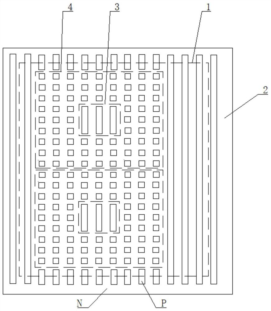
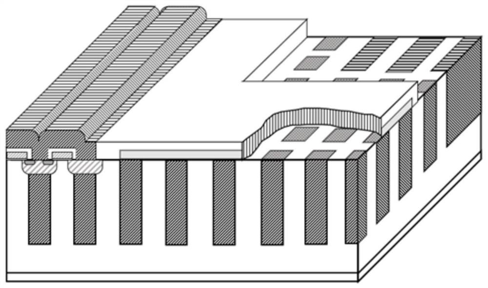
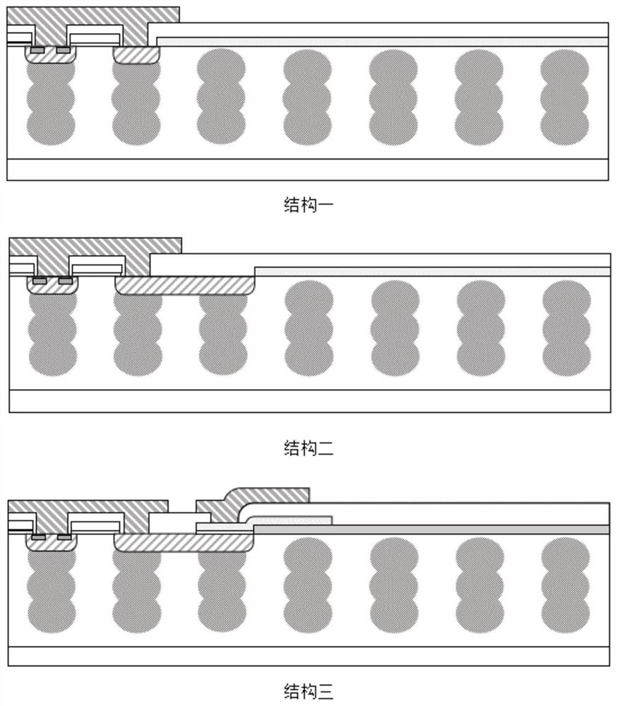
[0042] The invention provides an intelligent super junction MOS device, such as figure 1 and 2 As shown, it includes the main MOS and several functional MOSs integrated and connected on one chip, and the functional MOSs include sampling MOSs and / or startup MOSs.

[0043] The distribution of the main MOS on the chip includes the main MOS terminal area 2 and the main MOS active area 1 set inside the main MOS terminal area 2; the functional MOS is set within the scope of the main MOS active area 1, and the main MOS terminal area 2 and The main MOS active region 1 respectively includes several groups of P-type doped region pillars and N-type doped region pillars arranged in parallel and spaced apart;

[0044] Several functional MOSs are arranged adjacent to each other, and the distribution of functional MOSs on the chip includes functional MOS isolation region...


PUM

PropertyMeasurementUnit
electrical resistivityaaaaaaaaaa
thicknessaaaaaaaaaa
thicknessaaaaaaaaaa

Abstract

The invention relates to the field of intelligent super-junction MOS devices, and discloses an intelligent super-junction MOS device and a manufacturing method thereof. According to the invention, the intelligent super-junction MOS device comprises a main MOS and a plurality of functional MOS which are integrally connected on a chip, and the intelligent super-junction MOS device is characterized in that the functional MOS is arranged in the range of the main MOS, the distribution of the functional MOS on the chip comprises a functional MOS isolation region and a functional MOS active region, and the functional MOS active region comprises a plurality of groups of P-type doped region columns and N-type doped region columns which are parallel to each other and are arranged at intervals. The functional MOS isolation region comprises N-type doped region columns and P-type doped region columns, the N-type doped region columns surround the periphery of the functional active region in a square shape, and the P-type doped region columns are evenly distributed in the N-type doped region columns in a lattice shape. According to the intelligent super-junction MOS device disclosed by the invention, the independence of a functional MOS active region can still be ensured after process high-temperature annealing, and ultrahigh isolation voltage can be ensured.

Description

technical field [0001] The invention relates to the field of intelligent super junction MOS devices, more specifically, it relates to an intelligent super junction MOS device and a manufacturing method thereof. Background technique [0002] Intelligent super junction MOS device products are based on ordinary super junction products, integrating sampling MOS, startup MOS, high resistance R, or only integrating one of sampling MOS and startup MOS, ordinary super junction and smart super junction For circuit diagrams, see Figure 13 . It can be seen that the intelligent super-junction MOS device products will have 2 to 3 MOSs on the same chip, and the application circuit requires that the functions of the MOSs are independent and do not affect each other in the working state; [0003] Super junction products are composed of multiple sets of P-type doped region columns and N-type doped region columns alternately connected. Therefore, in the isolation design of sampling MOS and ...

Claims


Application Information

Patent Timeline
Patent Type & Authority Applications(China)
IPC IPC(8): H01L27/088H01L29/06H01L21/8234
CPCH01L27/088H01L21/823481H01L29/0634H01L29/0692
Inventor 翟士杰何军胡兴正薛璐
Owner 滁州华瑞微电子科技有限公司
Why Eureka
Try Eureka