Automatic die bonder for semiconductor chip processing
A technology of semiconductor and die bonding machine, applied in semiconductor/solid-state device manufacturing, electrical components, circuits, etc., can solve the problems of cumbersome operation and uneven dispensing, and achieve the effect of ensuring quality, easy operation and improving processing efficiency
- Summary
- Abstract
- Description
- Claims
- Application Information
AI Technical Summary
Problems solved by technology
Method used
Image

Examples
Embodiment Construction
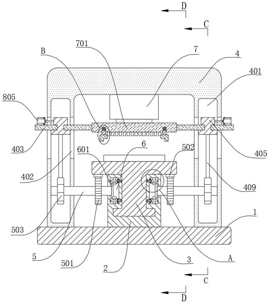
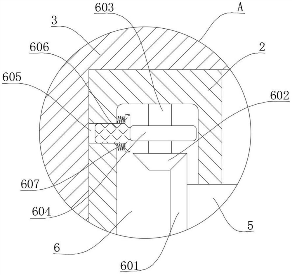
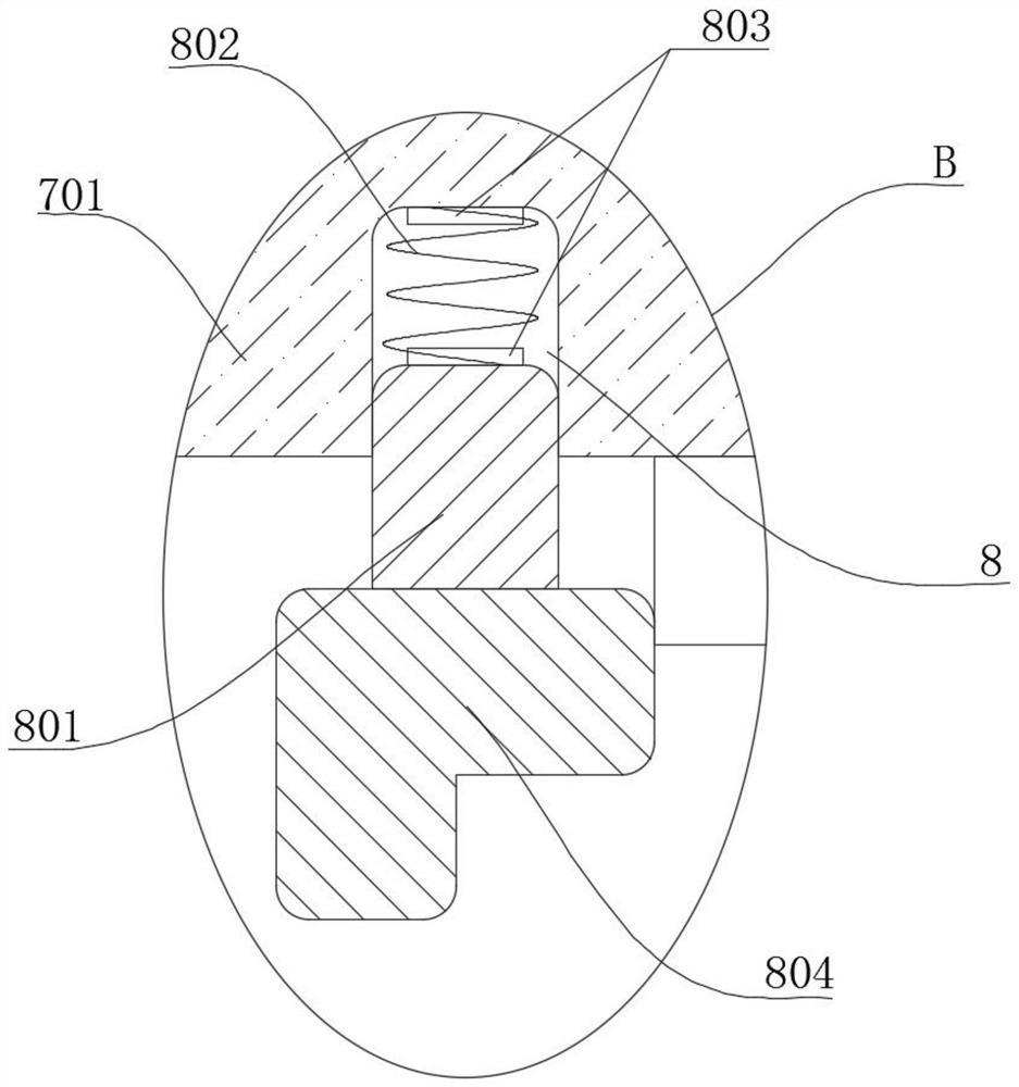
[0028] refer to Figure 1-8 , an automatic die bonding machine for semiconductor chip processing, including a base 1, the upper surface of the base 1 is fixedly connected with a slide rail 2, and the slide rail 2 is slidably connected with a sliding seat 3, such as figure 1 As shown, the cross-section of the sliding seat 3 is I-shaped, and the upper surface of the sliding seat 3 is provided with a chip tray, a processing tray, and a tin plastic tray, and its setting direction is as follows: figure 1 Arranged from right to left, the upper surface of base 1 is fixedly connected with U-shaped beam 4, the lower surface of U-shaped beam 4 is fixedly connected with electric push rod 7, the lower surface of the horizontal part of electric push rod 7 is fixedly connected with electric push rod 7, and the electric push rod 7 The output end of the rod 7 is fixedly connected with a vacuum block 701. A vacuum cavity is arranged in the vacuum block 701, and a vacuum suction head is provide...
PUM
 Abstract
Description
Claims
Application Information
 - R&D Engineer
- R&D Manager
- IP Professional
- Industry Leading Data Capabilities
- Powerful AI technology
- Patent DNA Extraction
Browse by: Latest US Patents, China's latest patents, Technical Efficacy Thesaurus, Application Domain, Technology Topic.
© 2024 PatSnap. All rights reserved.Legal|Privacy policy|Modern Slavery Act Transparency Statement|Sitemap