

Three-dimensional circuit manufacturing process and composite components of laser plastic material and manufacturing method
A technology of three-dimensional circuit and manufacturing process, which is applied in the fields of printed circuit manufacturing, cable/conductor manufacturing, circuit, etc. It can solve the problems that the three-dimensional circuit assembly technology has not been rapidly promoted, the microstructure is not smooth, and the appearance is affected, and the sintering time is shortened. , increase the speed, reduce the effect of concentration polarization
- Summary
- Abstract
- Description
- Claims
- Application Information
AI Technical Summary
Problems solved by technology
Method used
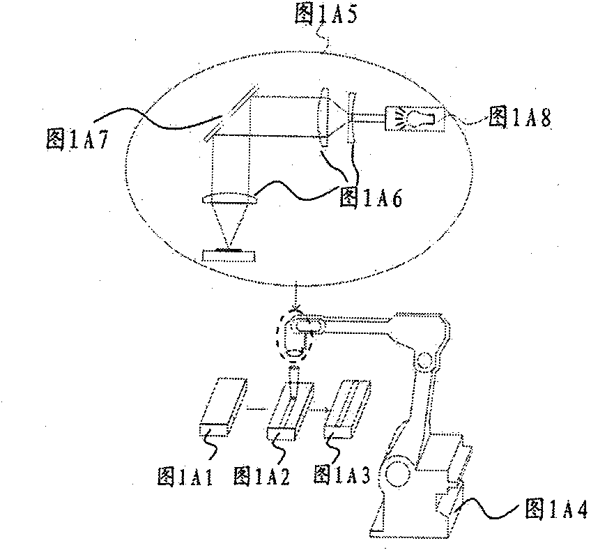
Image

Examples
Embodiment 1
[0094] Implementation example 1: Active GPS plastic antenna
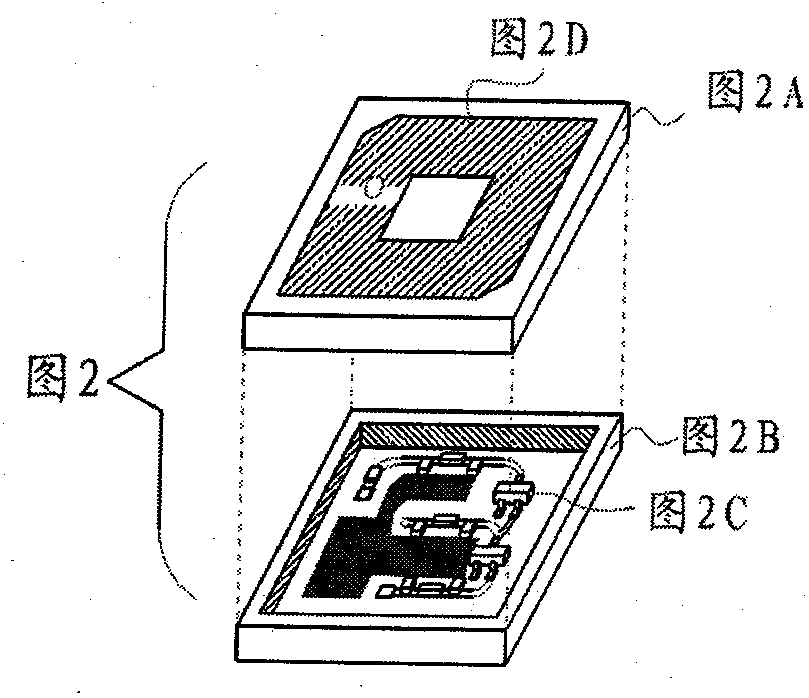
[0095] Such as figure 2 As shown, the active antenna consists of the antenna ( figure 2 A and figure 2 D) Add antenna amplification part ( figure 2 C) composition, antenna metal pattern ( figure 2 D) Arranged on the laser plastic with polyethylene (PE) or syndiotactic polystyrene (SPS) as the carrier masterbatch ( figure 2 A), the composite components in the carrier masterbatch are: 1-10 grams of surfactant; 5-200 grams of compatibilizer; 0.1-5 grams of light absorber; 0.5-30 grams of viscosity reducer; 5-750 grams of inorganic filler ; Modified organometallic compound 30-50 grams; the rest is carrier masterbatch. The sum of the composite ingredients must meet 100%.
[0096] The three-dimensional circuit manufacturing process is adopted, and the laser machine adopts near-infrared laser (1064nm) or ultraviolet laser scanning; then rapid chemical copper plating; finally, the lead wire and the amplifier cir...
Embodiment 2
[0098] Implementation example 2: multi-faceted high-power LED plastic lamp holder
[0099] The traditional LDE lamp holder is a ceramic base, which is made by sintering the terminal electrodes on the insulating ceramic sheet, and then chemically plating copper, nickel, and gold by using the traditional chip ceramic resistance-capacitance process. Ceramic technology cannot produce complex polyhedral shapes.
[0100] However, the luminous feature of LED lights is direct light. Generally, high-power lights are composed of several LEDs. In order to make the light source distributed in the hemispherical space, such as image 3 As shown, the ideal arrangement of LED lights ( image 3 The method of A) is polyhedron arrangement, and heat-conductive laser plastic molding or injection molding into a plastic base ( image 3 B).
[0101] The example of the present invention uses a heat-conducting laser plastic material as a component: the carrier masterbatch is CBT, and the composite c...
Embodiment 3
[0104] Implementation Example 3: Applications in Automobiles, Aircraft and Other Fields
[0105] Cars, airplanes, train carriages, etc. have large plastic parts and a large number of cables need to be arranged to transmit various electronic signals. Traditional cables are combined with plastics through bolts, screws and hardware, which are heavy and easy to use during exercise. For products that are particularly sensitive to weight, such as aircraft, it is a very good measure to use the three-dimensional circuit technology of the present invention to pre-embed a large number of signal lines in plastic parts, which not only reduces the failure rate but also reduces weight, and easy to maintain. The main function of plastics used in automobiles is to reduce the weight of automobiles, so as to achieve the purpose of fuel saving and high speed. Developed countries regard the amount of plastic used in automobiles as an important symbol to measure the level of automobile design and...
PUM
| Property | Measurement | Unit |
|---|---|---|
| Diameter | aaaaa | aaaaa |
| Thickness | aaaaa | aaaaa |
Abstract
Description
Claims
Application Information