Supercharge Your Innovation With Domain-Expert AI Agents!

OLED display panel and manufacturing method thereof

A display panel and manufacturing method technology, applied in semiconductor/solid-state device manufacturing, electrical components, electric solid-state devices, etc., can solve problems such as brightness and color gamut loss, loss of energy, and viewers cannot obtain viewing effects, etc., to achieve improved display Color gamut, reduce work energy consumption, improve the effect of display brightness

Pending Publication Date: 2021-10-29
SHENZHEN CHINA STAR OPTOELECTRONICS TECH CO LTD
View PDF5 Cites 0 Cited by
  • Summary
  • Abstract
  • Description
  • Claims
  • Application Information

AI Technical Summary

Problems solved by technology

[0005] While the display light 03 is being refracted, part of the display light 03 continues to penetrate the glass substrate 02, and becomes the display light 03' into the viewer's field of view; the other part of the display light 03 will Reflected by the glass substrate 02, the display light 03" is reflected back into the OLED light-emitting layer, and cannot enter the viewer's field of view
[0006] Compared with the display light 03, the display light 03' passing through the glass substrate 02 has already lost some energy, which means that the light extraction efficiency of the OLED display panel is not ideal
Therefore, in the conventional technology, in order to make the OLED display panel reach the required target brightness, it needs to pay more energy consumption to drive the OLED light-emitting layer 01 to emit the display light 03 with higher energy; or, in Under the requirement of limited energy consumption, the brightness and color gamut of the OLED display panel will be reduced, so that the viewer cannot obtain the expected viewing effect

Method used


Image

  • OLED display panel and manufacturing method thereof
  • OLED display panel and manufacturing method thereof
  • OLED display panel and manufacturing method thereof

Examples


Embodiment Construction

[0030] In order to make the above and other objects, features and advantages of the present invention more comprehensible, preferred embodiments of the present invention will be exemplified below in detail with accompanying drawings.

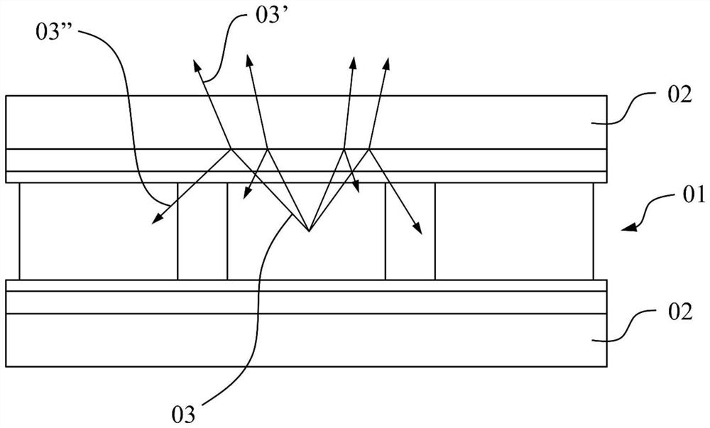
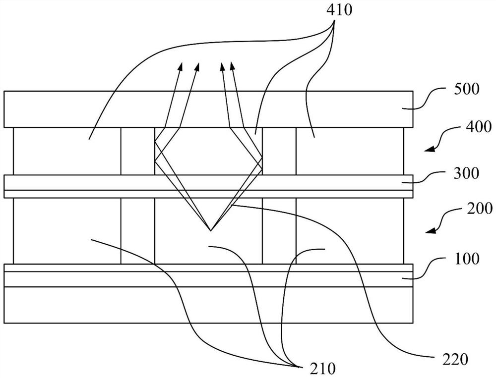
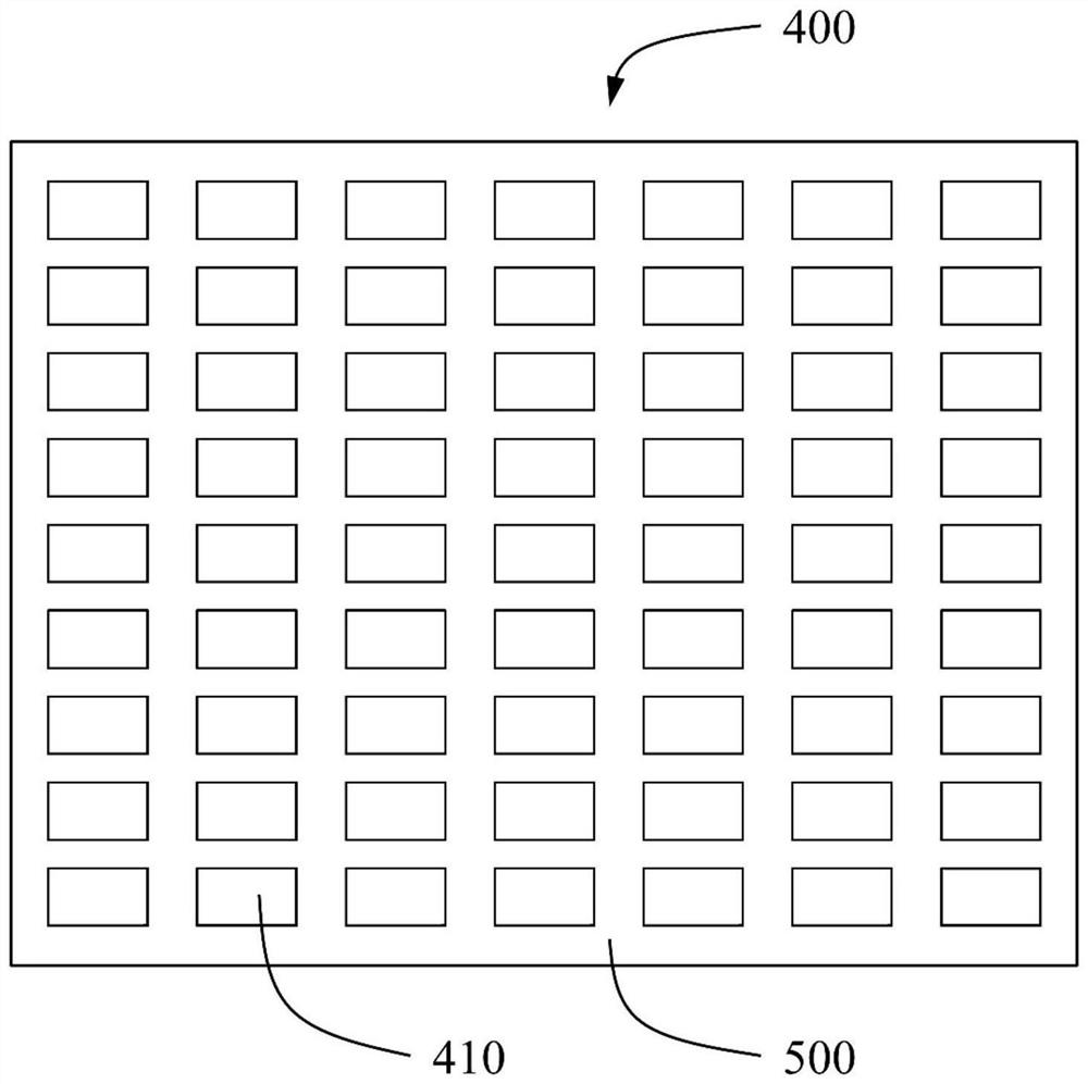
[0031] The invention provides an organic light-emitting diode (OLED) display panel. Please refer to figure 2 , which is a schematic structural view of the OLED display panel of the present invention. The OLED display panel includes a first electrode layer 100 , an OLED light emitting layer 200 , a second electrode layer 300 , and a light extraction layer 400 .

[0032] The OLED light emitting layer 200 is disposed on the first electrode layer 100 and includes a plurality of pixels 210 . It should be noted that, in one embodiment, the plurality of pixels 210 may be individual pixel points of the OLED display panel; in another embodiment, each of the plurality of pixels 210 may also include a plurality of sub-pixels , such as red sub-pixels, g...


PUM

PropertyMeasurementUnit
Thicknessaaaaaaaaaa

Abstract

The invention provides an organic light-emitting diode (OLED) display panel and a manufacturing method of the OLED display panel. The OLED display panel includes a first electrode layer, an OLED light-emitting layer, a second electrode layer, and a light extraction layer. The OLED light-emitting layer is arranged on the first electrode layer and comprises a plurality of pixels. And the second electrode layer is arranged on the OLED light emitting layer. The light extraction layer is arranged on the second electrode layer and comprises a plurality of light extraction columns. Each of the plurality of light extraction columns is disposed corresponding to each of the plurality of pixels. When display light emitted by each of the plurality of pixels enters each of the plurality of light extraction columns, the display light is totally reflected in each of the plurality of light extraction columns and is emitted from one side of each of the plurality of light extraction columns back to each of the plurality of pixels.

Description

technical field [0001] The invention relates to the field of display technology, in particular to an OLED display panel and a manufacturing method thereof. Background technique [0002] Organic light-emitting diode (OLED) display panels have advantages such as wide viewing angle and wide color gamut, and are concerned and developed by major display device manufacturers as mainstream display panels. However, since the refractive index of the glass substrate in the OLEED display panel is different from that of the OLED light emitting layer in the OLED display panel, part of the display light emitted by the OLED light emitting layer will be reflected back into the OLED light emitting layer. Part of the display light cannot be emitted from the OLED display panel, resulting in a low light extraction rate of the OLED display panel. [0003] Please refer to figure 1 , which is a schematic structural diagram of an OLED display panel in the prior art. The OLED display panel includ...

Claims


Application Information

Patent Timeline
IPC IPC(8): H01L51/52H01L51/56H01L27/32
CPCH10K59/00H10K50/85H10K71/00
Inventor 宋媛媛
Owner SHENZHEN CHINA STAR OPTOELECTRONICS TECH CO LTD
Features
  • R&D
  • Intellectual Property
  • Life Sciences
  • Materials
  • Tech Scout
  • Unparalleled Data Quality
  • Higher Quality Content
  • 60% Fewer Hallucinations
Learn More