

Display device and bonding method thereof, and display equipment
A display device and display panel technology, applied in the direction of identification devices, instruments, etc., can solve problems affecting the accuracy of bonding equipment, and achieve the effects of improving bonding accuracy and correcting differences in expansion
- Summary
- Abstract
- Description
- Claims
- Application Information
AI Technical Summary
Problems solved by technology
Method used
Image

Examples
Embodiment 1
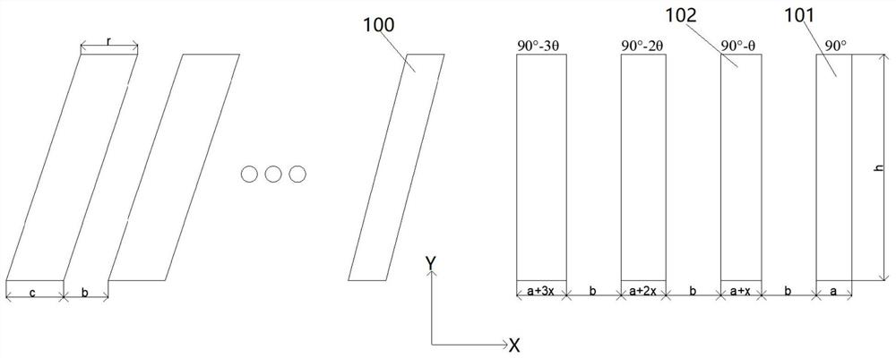
[0070] display panel
[0071] Please refer to figure 1 , the display panel is provided with a plurality of mutually independent first pins arranged along the first direction X, and the plurality of first pins include a first center pin located on the center line of the display panel and a first pin located on the first A number of first side pins on both sides of the central pin, the axes of the first side pins are set at an angle with the center line of the display panel; wherein, the arrangement direction from the first central pin to both sides Above, the first spacing between adjacent sides of two adjacent first pins is equal, and the width of the first pins increases sequentially.
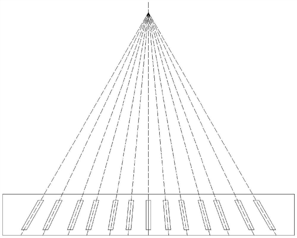
[0072] When specifically setting the shape of the first pin, the first pin (which may also be referred to as a panel pin in the following description) can be arranged axisymmetrically with respect to the axis of the first pin, and when specifically setting the first pin In addition, the sh...
Embodiment 2
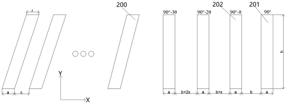
[0088] drive carrier
[0089] Please refer to figure 2 , the driving carrier is provided with a plurality of second pins corresponding to each of the first pins one by one, and the plurality of second pins include a second center pin located on the center line of the display panel and a second pin located on the center line of the display panel. A number of second side pins on both sides of the second central pin, the axes of the second side pins are set at an angle with the center line of the display panel; wherein, from the second central pin to the two sides In the arrangement direction, the widths of the second pins are equal, and the second spacing between adjacent sides of two adjacent second pins increases sequentially.
[0090] Such as figure 2 As shown, in the embodiment of the present application, it is assumed that the width of the second central pin is a, and the distance between the second central pin and the adjacent second side pin is b. It should be note...
PUM
 Abstract
Description
Claims
Application Information