

Wafer assembly
A technology of wafers and components, applied in the direction of electrical components, electrical solid devices, semiconductor devices, etc., can solve problems affecting the efficiency and accuracy of wafer bonding recognition, small pattern size, etc., to improve recognition efficiency and accuracy, improve key Combined precision, the effect of large chip effective area
- Summary
- Abstract
- Description
- Claims
- Application Information
AI Technical Summary
Problems solved by technology
Method used
Image

Examples
Embodiment Construction
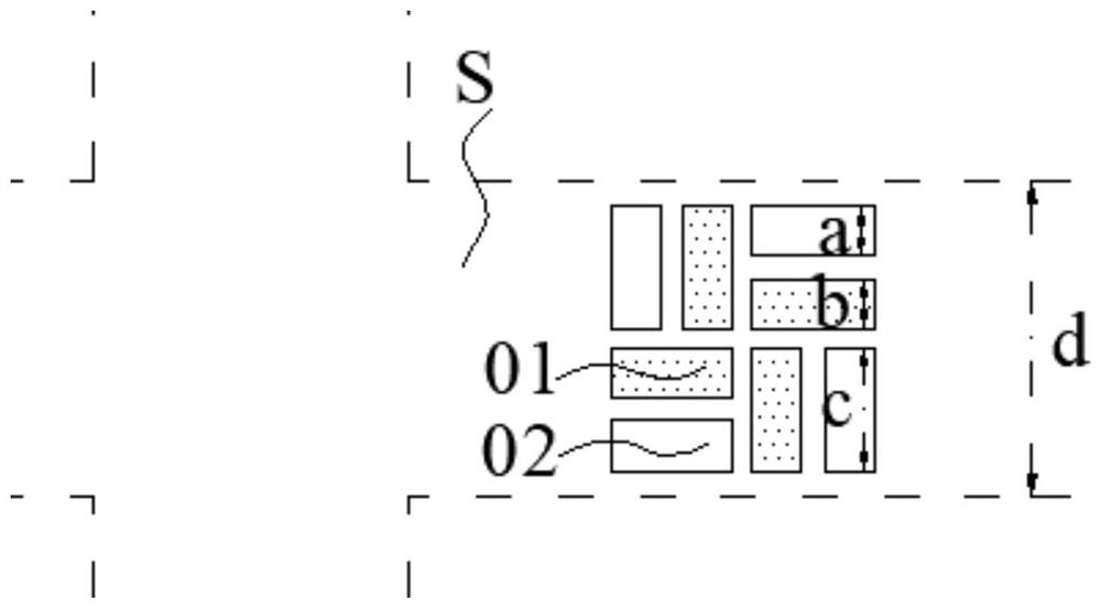
[0033] As mentioned in the background art, as the width of dicing lines in 3D-IC design becomes smaller and smaller, the size of the patterns left for alignment marks is bound to become smaller, which affects the efficiency and accuracy of wafer bonding recognition. Specifically, such as figure 1 As shown, the wafer assembly includes two wafers, one wafer includes an alignment mark 01, and the other wafer includes an alignment mark 02, and the alignment mark 01 and the alignment mark 02 are matched for the pairing of the two wafers. allow. The line width of the alignment mark 01 is b, the line width of the alignment mark 02 is a, and the line length of the alignment mark 02 is c. The width d of the scribe line S itself is getting smaller and smaller. The line width a of the alignment mark 02 plus the line width b of the alignment mark 01 plus the line length c of the alignment mark 02 must be smaller than the width d of the scribe line, that is, a+ b+c<d. In this way, the w...
PUM
 Abstract
Description
Claims
Application Information