Pixel structure, preparation method thereof and display panel
A technology of pixel structure and scattering structure, which is applied in the direction of instruments, electrical components, electric solid devices, etc., can solve the problem that the color conversion structure of the pixel structure is easy to be damaged, so as to maximize the utilization rate, improve the yield rate, and maximize the luminous efficiency Effect
- Summary
- Abstract
- Description
- Claims
- Application Information
AI Technical Summary
Problems solved by technology
Method used
Image


Examples
preparation example Construction
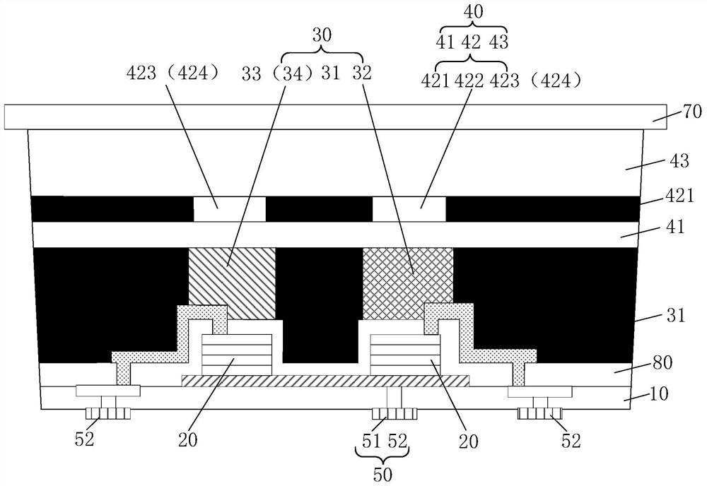
[0119] Optionally, the method for preparing the pixel structure further includes: preparing a second protective layer on the side of the substrate 10 away from the electrode layer 50 , on the side of each micro-luminescent crystal 20 away from the substrate 10 , and on the side of each micro-luminescent crystal 20 80 , and the dimming layer 30 is prepared on the side of the second protective layer 80 away from the substrate 10 and each micro light-emitting crystal grain 20 away from the substrate 10 .
[0120] Optionally, the aforementioned step S130: preparing the light filter layer 40 on the side of the light-adjusting layer 30 away from the substrate includes: preparing the first encapsulation layer 41 on the side of the light-adjustment layer 30 away from the substrate, and the first encapsulation layer 41 A second light-shielding layer is prepared on the side away from the light-adjusting layer 30, and the second light-shielding layer is patterned to obtain a second light-...
PUM
| Property | Measurement | Unit |
|---|---|---|
| thickness | aaaaa | aaaaa |
| thickness | aaaaa | aaaaa |
| thickness | aaaaa | aaaaa |
Abstract
Description
Claims
Application Information