Eureka AIR delivers breakthrough ideas for toughest innovation challenges, trusted by R&D personnel around the world.

OLED display panel and OLED display device

A technology for display panels and display devices, applied in the fields of instruments, electrical digital data processing, electrical components, etc., can solve the interference between touch signals and display signals, affect the display effect and touch effect, and mutual interference between touch signals and display signals and other problems to achieve the effect of avoiding parasitic capacitance and avoiding interference

Active Publication Date: 2021-12-03
WUHAN CHINA STAR OPTOELECTRONICS SEMICON DISPLAY TECH CO LTD
View PDF7 Cites 0 Cited by
  • Summary
  • Abstract
  • Description
  • Claims
  • Application Information

AI Technical Summary

Problems solved by technology

However, since the transmission signal line and the reception signal line of the touch layer are connected to the signal terminals on the lower side of the display panel through both sides, and there is a display signal line between the transmission signal line and the reception signal line, resulting in a gap between the touch signal line and the display signal line. There is a parasitic capacitance between them, which will cause interference between the touch signal and the display signal, affecting the display effect and touch effect
[0003] Therefore, the existing Oncell display device has the technical problem of mutual interference between the touch signal and the display signal caused by the parasitic capacitance between the touch signal line and the display signal line.

Method used


Image

  • OLED display panel and OLED display device
  • OLED display panel and OLED display device
  • OLED display panel and OLED display device

Examples


Embodiment Construction

[0045]The technical solutions in the embodiments of the present application will be clearly and completely described below in conjunction with the drawings in the embodiments of the present application. Apparently, the described embodiments are only some of the embodiments of this application, not all of them. Based on the embodiments in this application, all other embodiments obtained by those skilled in the art without making creative efforts belong to the scope of protection of this application.

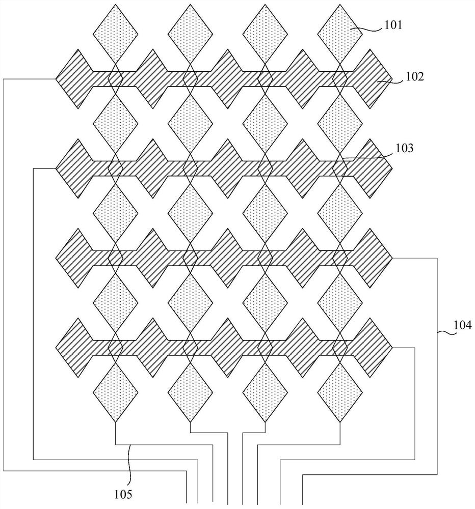
[0046] like figure 1 As shown, in the existing Oncell display device, the touch electrodes include receiving electrodes 102 arranged continuously in the horizontal direction and emitting electrodes 101 arranged in the vertical direction, and the emitting electrodes 101 are connected through a conductive bridge 103 of another layer. function, connect the receiving electrode 102 through the first metal wiring 104, connect the transmitting electrode 101 through the second metal wiri...


PUM


Abstract

The invention provides an OLED display panel and an OLED display device. According to the OLED display panel, a touch binding terminal and a display binding terminal are arranged in two areas respectively, a touch binding terminal area is arranged outside the display binding terminal area, so that the touch binding terminal and the display binding terminal do not intersect; meanwhile, a touch signal line is connected with the touch binding terminal on one side corresponding to the touch binding terminal area, and the display signal lines are connected with the display binding terminals on the side corresponding to the display binding terminal area, so that the touch signal lines and the display signal lines do not intersect, stray capacitance between the touch signal lines and the display signal lines can be avoided, and interference between touch signals and display signals is avoided.

Description

technical field [0001] The present application relates to the field of display technology, in particular to an OLED display panel and an OLED display device. Background technique [0002] With the development of display technology, in the existing mutual-capacitance Oncell (the touch layer is arranged between the light-emitting layer and the polarizer) OLED (Organic Light-Emitting Diode, organic light-emitting diode) display screen, the touch layer is arranged on the on the encapsulation layer to reduce the thickness of the display panel. Oncell display devices set the touch electrodes on the packaging layer, and the metal traces connecting the touch electrodes extend down to the signal terminals on both sides of the binding area through both sides, and then connect the touch chips with the signal terminals to realize touch control. function, and the driving circuit realizes the driving function by connecting with the driving chip, thereby realizing the touch control and dr...

Claims


Application Information

Patent Timeline
IPC IPC(8): H01L27/32G06F3/041G06F3/044
CPCG06F3/0412G06F3/0445G06F3/0446G06F2203/04111H10K59/40H10K59/131
Inventor 叶剑梁鹏飞
Owner WUHAN CHINA STAR OPTOELECTRONICS SEMICON DISPLAY TECH CO LTD
Why Eureka
Eureka Blog
Learn More