Three-dimensional NAND memory device structure and preparation method thereof

A storage device, three-dimensional technology, applied in the field of memory, can solve problems such as damage to the top layer structure, lower structural yield of three-dimensional NAND storage devices, reliability failure, etc., and achieve the effect of low process complexity

Active Publication Date: 2020-07-10
YANGTZE MEMORY TECH CO LTD
View PDF6 Cites 11 Cited by
  • Summary
  • Abstract
  • Description
  • Claims
  • Application Information

AI Technical Summary

Problems solved by technology

[0006] However, in the process of forming channel holes by using the above multiple stacks, due to the influence of stress and other factors, there will be overlay deviations in the photoresist layer between the channel holes in the upper stack and the channel holes in the lower stack. When the SONO at the bottom of the channel is opened to form a circuit loop between the substrate well layer (usually P well) and the channel layer, it will cause the top layer structure at the lower end of the upper channel hole at the layer-to-layer connection (that is, ONO) Damaged, which reduces the yield rate and reliability failure of the three-dimensional NAND memory device structure

Method used


Image

  • Three-dimensional NAND memory device structure and preparation method thereof
  • Three-dimensional NAND memory device structure and preparation method thereof
  • Three-dimensional NAND memory device structure and preparation method thereof

Examples


Embodiment 1

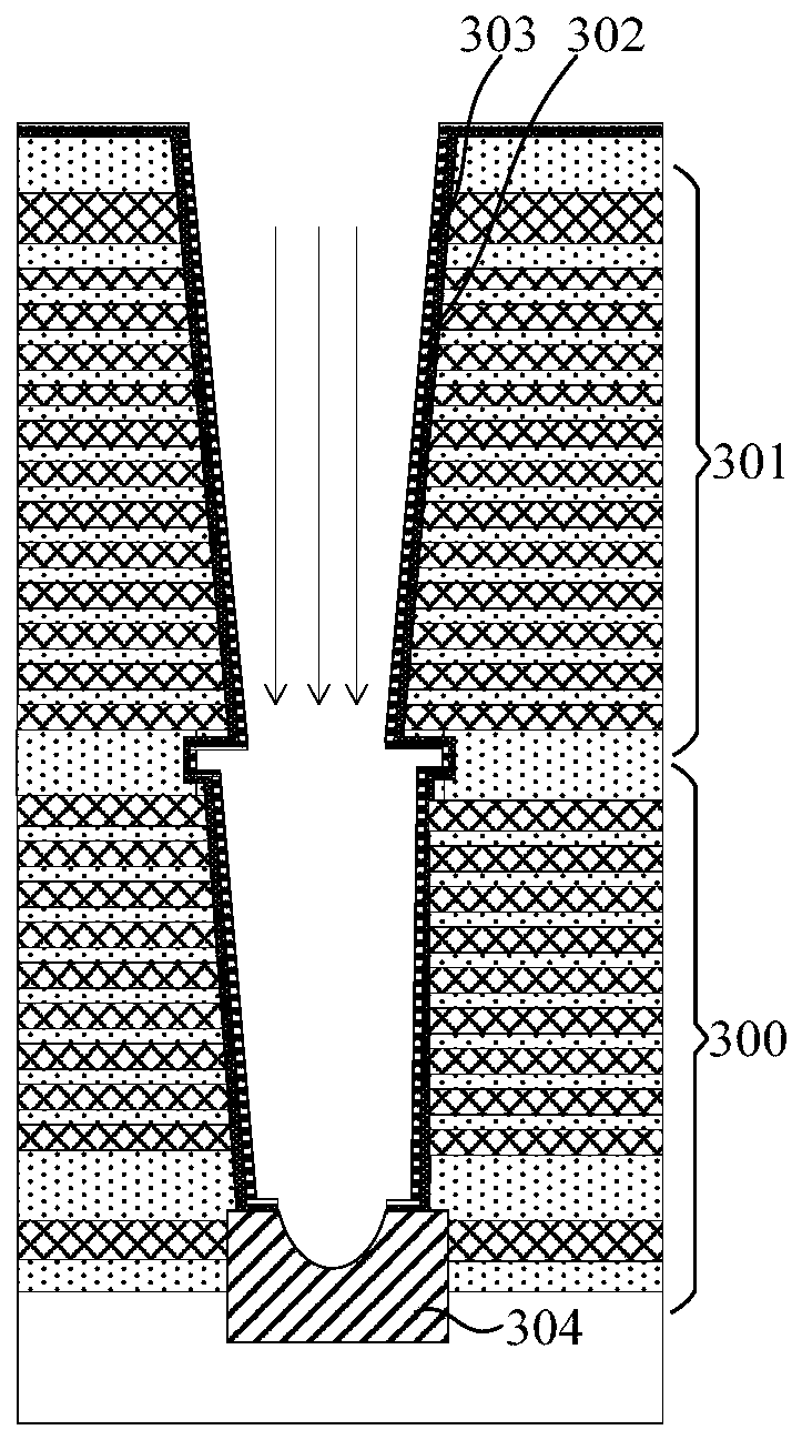
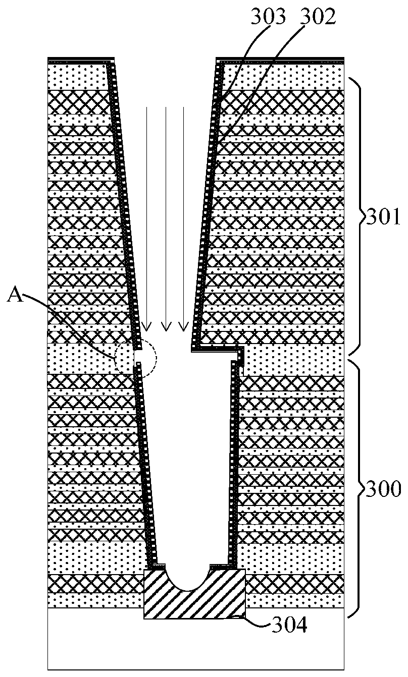
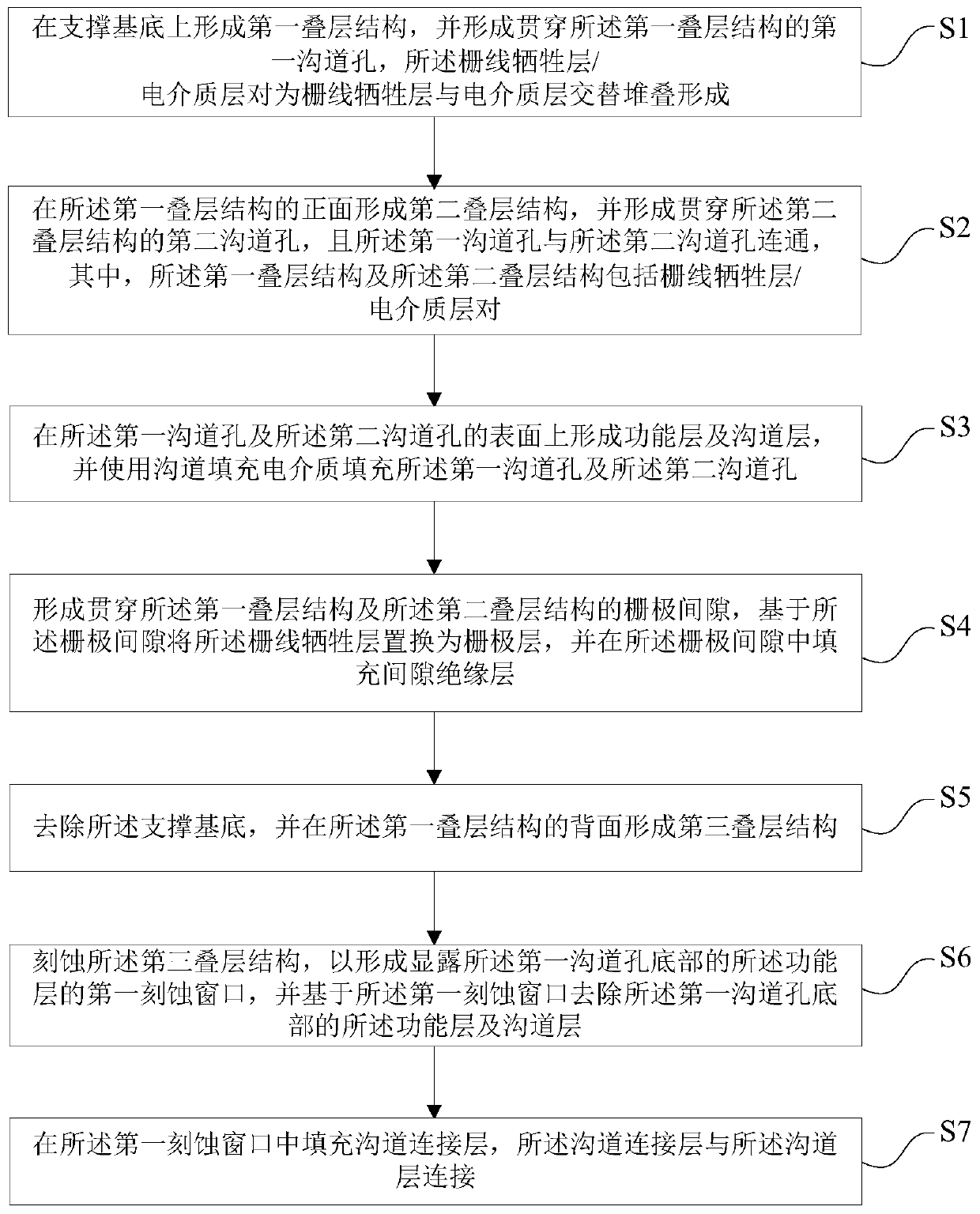
[0126] like image 3 As shown, in order to solve the above problems, this embodiment provides a method for preparing a three-dimensional NAND memory device structure, including the following steps:

[0127] like image 3 , Figure 4 to Figure 6As shown, step S1 is firstly performed to form a first laminated structure 101 of a grid line sacrificial layer 105 / dielectric layer 106 pair on a support substrate 100 (such as Figure 4 ), and form a first channel hole 102 penetrating through the first stacked structure 101 (as shown in Figure 5 shown).

[0128] As an example, the gate line sacrificial layer 105 may be a nitride layer, such as silicon nitride; the dielectric layer 106 may be an oxide layer, such as silicon oxide.

[0129] The first stacked structure 101 may include any suitable number of gate line sacrificial layer 105 / dielectric layer 106 pairs. In some embodiments, the total number of gate line sacrificial layer 105 / dielectric layer 106 pairs in the first stac...

Embodiment 2

[0171] This embodiment provides a three-dimensional NAND storage device structure, which can be prepared by the preparation method of the first embodiment above, but is not limited to the preparation method described in the first embodiment, as long as the device structure can be formed. For the beneficial effects achieved by the device structure, please refer to Embodiment 1, which will not be described in detail below.

[0172] like Figure 25 As shown, the structure includes:

[0173] The substrate layer 200 has opposite front and back sides;

[0174] The fourth stacked structure 201 and the fifth stacked structure 202 stacked in sequence are located on the front side of the substrate layer 200, wherein the fourth stacked structure 201 and the fifth stacked structure 202 include a gate layer 203 / dielectric layer 204 pair, the gate layer 203 includes the storage gate layer of the storage transistor and the upper selection gate layer of the upper selection transistor;

[0...


PUM


Abstract

The invention provides a three-dimensional NAND memory device structure and a preparation method thereof. The method comprises the following steps: forming a first laminated structure and a second laminated structure with communicated channel holes on a support substrate; forming a functional layer, a channel layer and a filling dielectric on the surface of the channel hole; forming a gate gap; filling a gap insulating layer in the gate gap; removing the support substrate, and forming a third laminated structure on the back surface of the first laminated structure; etching the third laminatedstructure to form a first etching window, and removing the functional layer at the bottom of the first channel hole based on the first etching window; and filling a channel connection layer in the first etching window. The channel connection layer is formed at the corresponding position of the back surface of the channel hole, so that the risk that the functional layer at the connecting part of the upper channel hole and the lower channel hole is damaged when the channel connection layer and the channel layer are connected through a process of punching from the front surface of the channel hole is avoided; and in addition, the process for forming the channel connection layer is low in complexity, easy to control and high in yield.

Description

technical field [0001] The invention relates to the technical field of memory, in particular to a three-dimensional NAND memory device structure and a preparation method thereof. Background technique [0002] The computing environment paradigm has changed to ubiquitous computing systems that can be used anytime, anywhere. Due to this fact, the use of portable electronic devices such as mobile phones, digital cameras, and notebook computers has rapidly increased. These portable electronic devices usually use storage systems with storage devices, ie data storage devices. Data storage devices are used as primary or secondary storage devices in these portable electronic devices. Thus, the reliability and performance of digital data storage, such as storage systems, is critical. These data storage devices using memory devices offer excellent stability, durability, high information access speed, and low power consumption. Examples of data storage devices having these advantage...

Claims


Application Information

Patent Timeline
Patent Type & Authority Applications(China)
IPC IPC(8): H01L27/1157H01L27/11582
CPCH10B43/35H10B43/27Y02D10/00
Inventor 徐伟杨星梅王健舻吴继君黄攀周文斌
Owner YANGTZE MEMORY TECH CO LTD
Why Eureka
Try Eureka