Fin type field effect transistor and manufacture method thereof

A technology of fin field effect and manufacturing method, which is applied in semiconductor/solid-state device manufacturing, semiconductor devices, electrical components, etc., can solve problems affecting the electrical performance of fin field effect transistors, and achieve the goal of avoiding parasitic capacitance and good electrical performance Effect

Active Publication Date: 2013-06-19
SEMICON MFG INT (SHANGHAI) CORP
View PDF5 Cites 10 Cited by
  • Summary
  • Abstract
  • Description
  • Claims
  • Application Information

AI Technical Summary

Problems solved by technology

However, it has been found in practical applications that there is a large parasitic capacitance between the metal gate and the source / drain of the fin field effect transistor formed by the above manufacturing method, which seriously affects the electrical performance of the fin field effect transistor

Method used


Image

  • Fin type field effect transistor and manufacture method thereof
  • Fin type field effect transistor and manufacture method thereof
  • Fin type field effect transistor and manufacture method thereof

Examples


Embodiment Construction

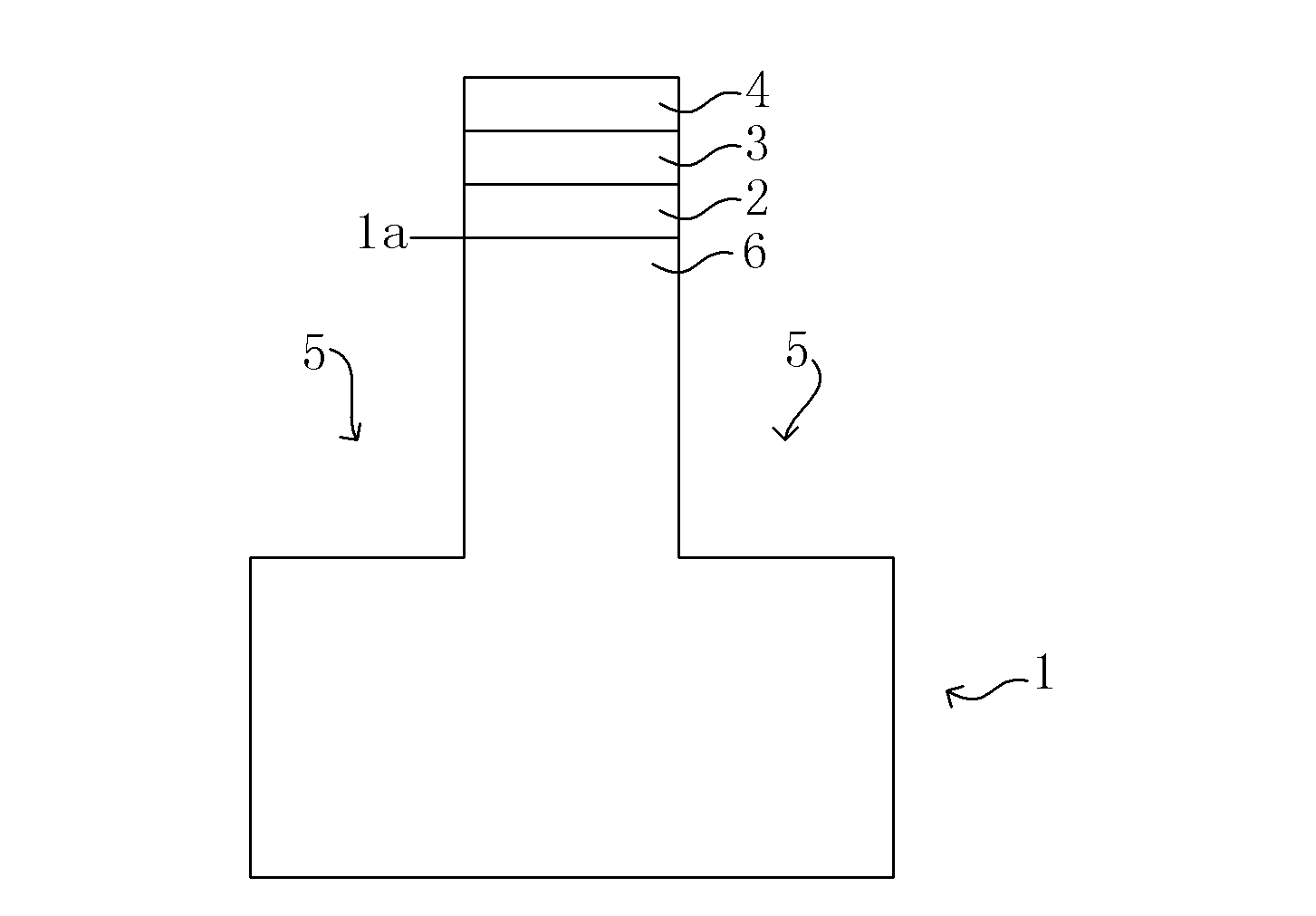
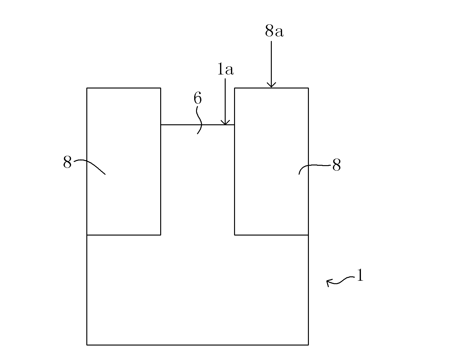
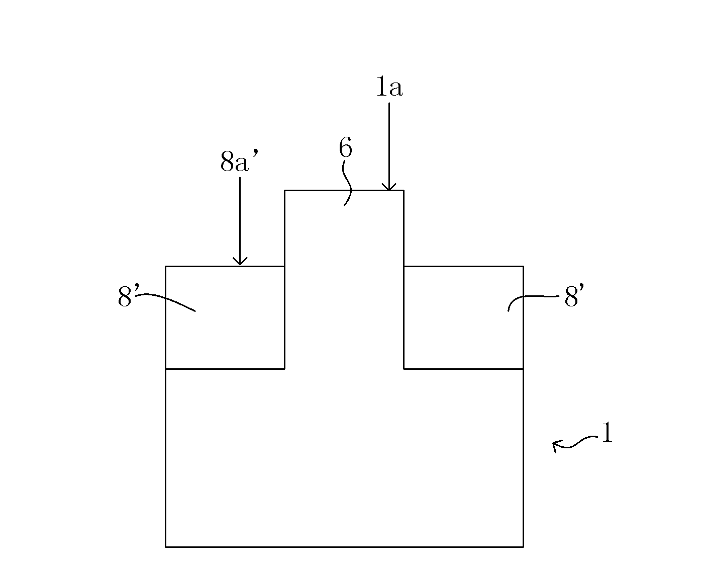
[0054] As mentioned in the background, there is a large parasitic capacitance between the metal gate and the source / drain of the fin field effect transistor in the prior art, which seriously affects the electrical performance of the fin field effect transistor. The inventor knows through analysis that the reason for this phenomenon is: as Figure 2D As shown, when using the gate-last process to form the metal gate 15 of the fin field effect transistor, although a higher-quality high-K gate dielectric layer 14 can be formed, while depositing the high-K gate dielectric layer 14, it will cause metal grid 15 both side walls ( Figure 2D Middle, left, and right vertical sidewalls) are attached with a high-K gate dielectric layer 14, which is a material with a large dielectric constant. In this fin field effect transistor structure, the metal gate 15, the source The / drain 16 and the high-K gate dielectric layer 14 generate parasitic capacitance with a large capacitance.

[0055] ...


PUM


Abstract

The invention provides a fin type field effect transistor and a manufacture method of the fin type field effect transistor. The method comprises the steps that a fin is formed on a semiconductor substrate, a virtual grid electrode is formed on the semiconductor substrate with the formed fin and stretches across the fin, first side walls are formed on two sides of the virtual grid electrode, ions are implanted in the fin so as to form a source electrode and a drain electrode of the fin type field effect transistor, the virtual grid electrode is eliminated, an opening is formed in the position of the virtual grid electrode, a high-K-grid medium layer and a metal grid electrode material layer are sequentially deposited so as to fill the opening, and a metal grid electrode is formed, and the first side walls and the high-K-grid medium layer on the side wall of the metal grid electrode are eliminated. According to the fin type field effect transistor, the high-K-grid medium layer on two sides of the metal grid electrode are effectively eliminated in sequence, stray capacitance is prevented from generating between the metal grid electrode and the source electrode or the drain electrode, other semiconductor structures are prevented from being damaged during the eliminating process, and the fin type field effect transistor is enabled to be good in electrical properties.

Description

technical field [0001] The invention relates to the field of semiconductor integrated circuits, in particular to a fin field effect transistor and a manufacturing method thereof. Background technique [0002] Since the development of semiconductor integrated circuits, their performance has been steadily improving. Improvements in performance have been achieved primarily through the continued shrinking of the size of semiconductor components in integrated circuits. Among them, the CMOS transistor is a crucial semiconductor element. With the development of semiconductor technology, the feature size of CMOS transistors has shrunk to the 45nm node. But below the 45nm node, it is difficult to further develop the traditional planar CMOS technology, and new technologies must be produced in due course. Among the various technologies proposed, the multi-gate transistor technology is considered to be the most promising technology that can be applied after the sub-45nm node. Compar...

Claims


Application Information

Patent Timeline
Patent Type & Authority Applications(China)
IPC IPC(8): H01L21/336H01L21/28H01L29/78H01L29/423
Inventor 张海洋韩秋华
Owner SEMICON MFG INT (SHANGHAI) CORP
Why Eureka
Try Eureka