Integrated semiconductor light-emitting device and method for manufacturing same

a technology of integrated semiconductors and light-emitting devices, which is applied in the direction of semiconductor lasers, optical beam sources, semiconductor laser structural details, etc., can solve the problems of inability to obtain integrated semiconductor light-emitting devices, inability to use conventional direct bonding techniques to bond the first and second semiconductor light-emitting devices ldb>1/b> and ldb>2/b> together, and improve optical properties and electric properties. ,

Inactive Publication Date: 2005-08-11
PIONEER CORP
View PDF3 Cites 33 Cited by
  • Summary
  • Abstract
  • Description
  • Claims
  • Application Information

AI Technical Summary

Benefits of technology

[0033] The present invention has been made in light of the foregoing problems associated with the conventional art. It is therefore an object of the present invention to provide an integrated semiconductor light-emitting device and a manufacturing method thereof capable of enhancing mass productivity and improving the optical properties, the electric properties and the like.

Problems solved by technology

However, it is impossible to realize such integrated semiconductor light-emitting devices on the same substrate by the use of monolithic semiconductor manufacturing technology.
This limitation makes it impossible to obtain an integrated semiconductor light-emitting device because of the difficulty of using the conventional direct bonding technique to bond a laser wafer for producing the semiconductor light-emitting devices having an uneven bonding surface to another laser wafer in a construction thereof.
Hence, the bonding surface results in surface asperity, which in turn makes it impossible to use the conventional direct bonding techniques to bond the first and second semiconductor light-emitting devices LD1 and LD2 together.
In consequence, an integrated semiconductor light-emitting device using the GaN ridge-stripe laser is not able to be realized by the use of the conventional direct bonding techniques.
Thus, an increase in drive voltage and an increase in electrical power consumption are caused, leading to various problems such as the need to provide a large-sized heat dissipating structure.
If the integrated semiconductor light-emitting device having such positional relation between these two emission spots is mounted on the pickup, the following problem arises.
The comatic aberration thus caused with respect to the tangential direction t results in a deterioration of the quality of the optical spot.
However, the tilt correction mechanism is capable of making an angle adjustment only to the tilt in the radial direction r of the optical disc DCS, and has no angle adjustment mechanism for a tilt in the tangential direction t. For this reason, it is impossible to make a tilt correction to the light coming in at an angle with respect to the tangential direction t which is caused when the integrated semiconductor light-emitting device is located as described above.
In consequence, if the conventional integrated semiconductor light-emitting device is mounted on a regular pickup, a correction to the incident angle of the laser light S2 entering at an inclined angle with respect to the tangential direction t is impossible.
This results in further problem that the comatic aberration can not be reduced.

Method used


Image

  • Integrated semiconductor light-emitting device and method for manufacturing same
  • Integrated semiconductor light-emitting device and method for manufacturing same
  • Integrated semiconductor light-emitting device and method for manufacturing same

Examples


first embodiment

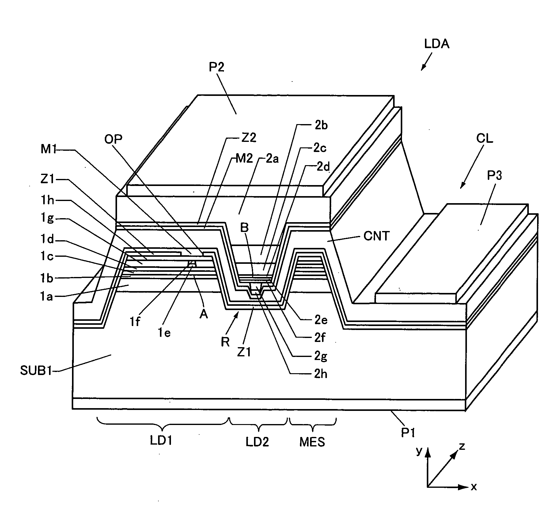
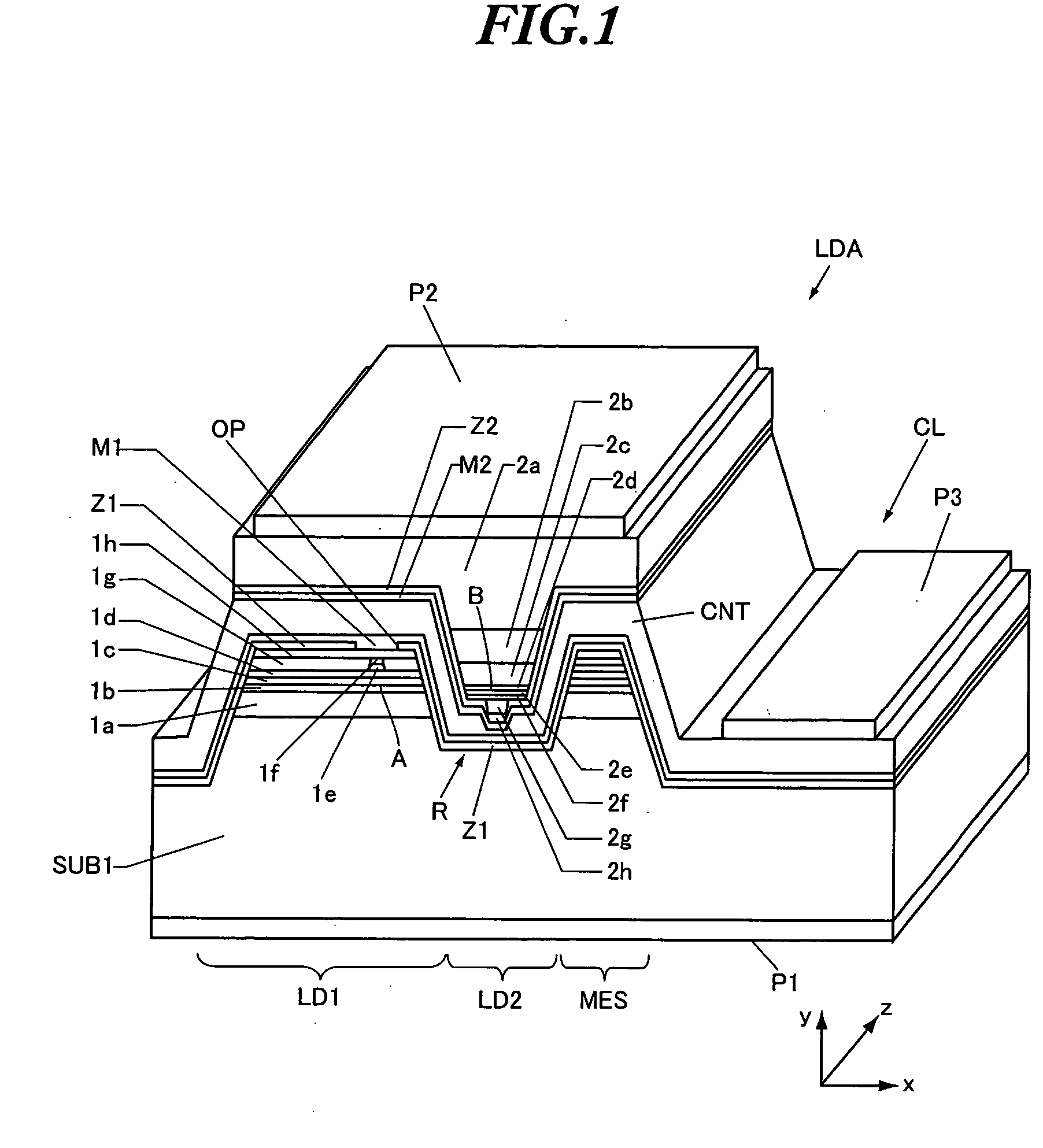
[0057]FIG. 1 shows an integrated semiconductor light-emitting device LDA having a first laser part LD1, a rise MES, a trench R formed between the first laser part LD1 and the rise MES, a stage CL adjacent to the rise MES, and a second laser part LD2. A metal bonding layer CNT is formed on the first laser part LD1, the trench R, the rise MES and the stage CL, and the second laser part LD2 is fitted into the trench R through the bonding layer CNT.

[0058] The horizontal direction (width direction) x of an MQW active layer 1b formed in the first laser part LD1 is substantially consistent with that of an MQW active layer 2d formed in the second laser part LD2.

[0059] The first laser part LD1 is formed of a II-VI compound semiconductor or a III-V compound semiconductor including any of arsenic (As), phosphorus (P) and antimony (Sb) as a group V element. The first laser part LD1 has an n-type cladding layer 1a, MQW active layer 1b, first p-type cladding layer 1c, p-type etch stopping layer...

second embodiment

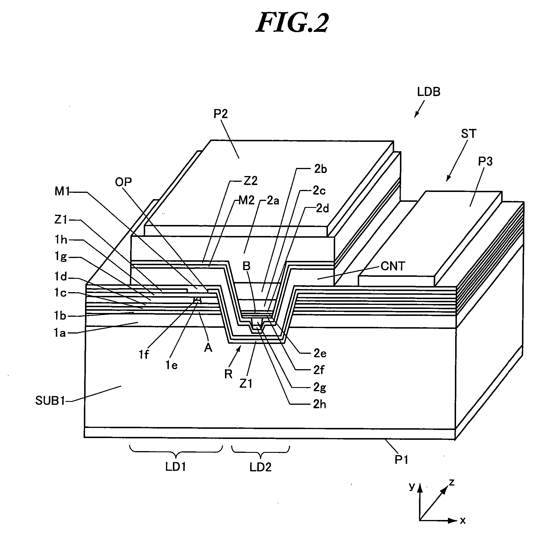
[0091] Next, an integrated semiconductor light-emitting device according to a second embodiment will be described with reference to FIG. 2. In FIG. 2, the same components as or corresponding components to those shown in FIG. 1 are designated with the same reference numerals as in FIG. 1.

[0092] In FIG. 2, the integrated semiconductor light-emitting device LDB has a first laser part LD1, a flat portion ST, a trench R formed in a hollow shape on the surfaces of the first laser part LD1 and the flat portion ST, and a projection-shaped second laser part LD2. The second laser part LD2 is fitted into the trench R through a metal bonding layer CNT. The first laser part LD1 and the flat portion ST have the flat surfaces of a table-like shape and are formed of a II-VI compound semiconductor or a III-V compound semiconductor including any of arsenic (As), phosphorus (P) and antimony (Sb) as a group V element. The projection-shaped second laser part LD2 is formed of a III-V compound semiconduc...

third embodiment

[0124] Next, a method for manufacturing the integrated semiconductor light-emitting device LDA illustrated in FIG. 1, according to the first embodiment of the present invention, will be described in detail with reference to FIGS. 4A to 6D as a third embodiment. FIGS. 4A to 6D are sectional views illustrating in the order of the steps of the manufacturing method for the integrated semiconductor light-emission device LDA, and the same components or regions as or the corresponding components or regions to those in FIG. 1 are designated with the same reference numerals as in FIG. 1.

[0125] In the third embodiment, a first laser wafer 100 with an n-type semiconductor substrate SUB1 on which a plurality of first laser parts LD1 are formed, and a second laser wafer 200 with a support substrate (e.g. sapphire substrate or AlN substrate) SUB2 on which a plurality of second laser parts LD2 are formed are prefabricated. The first and second laser wafers 100 and 200 are bonded together with a b...


PUM

PropertyMeasurementUnit
wavelengthaaaaaaaaaa

Abstract

An integrated semiconductor light-emitting device suitable for being mounted on a pickup is provided. The integrated semiconductor light-emitting device has a first laser part stacked on a semiconductor substrate and a projection-shaped second laser part formed by stack in thin-film-layer form. The second laser part is fitted into a trench formed adjacent to the first laser part in the semiconductor substrate. At least the first and second laser parts and the trench are bonded together through a metal bonding layer. An emission spot of the first laser part and an emission spot of the second laser part are located away in approximately the same horizontal direction perpendicular to the direction of the stack of the first and second laser parts.

Description

BACKGROUND OF THE INVENTION [0001] 1. Field of the Invention [0002] This invention relates to an integrated semiconductor light-emitting device which emits a plurality of laser lights of different wavelengths, and a method for manufacturing the integrated semiconductor light-emitting device. [0003] The present application claims priority from Japanese Application No. 2004-16023, the disclosure of which is incorporated herein by reference. [0004] 2. Description of the Related Art [0005] These days, mass digital contents have become easily available because of proliferation of a digital broadcast and broadband, and so there is a need for higher density information processing technology. [0006] For example, in the case of an optical disc used for recording / reproducing in an information recording / reproducing system such as a CD player and a DVD player, an increase in density from a CD (Compact Disc) with a capacity of 700 MB using a laser light with a wavelength of 780 nm band to a DVD ...

Claims


Application Information

Patent Timeline
Patent Type & Authority Applications(United States)
IPC IPC(8): H01S5/02G11B7/125H01S5/22H01S5/323H01S5/343H01S5/40
CPCH01S5/0202H01S5/0217H01S5/0224H01S5/02272H01S5/4087H01S5/32341H01S5/4031H01S5/405H01S5/32325H01S5/0234H01S5/0237
Inventor KIMURA, YOSHINORIMIYACHI, MAMORUCHIKUMA, KIYOFUMI
Owner PIONEER CORP
Why Eureka
Try Eureka