Packaging structure of capacitive fingerprint sensor

A fingerprint sensor and packaging structure technology, which is applied in the field of semiconductor capacitive fingerprint sensor packaging structure, can solve the problems of difficult machine assembly, increased packaging difficulty, increased cost, etc., and achieves low cost, easy large-scale production, and simple packaging process Effect

Active Publication Date: 2014-06-25
成都费恩格尔微电子技术有限公司 +1
View PDF7 Cites 63 Cited by
  • Summary
  • Abstract
  • Description
  • Claims
  • Application Information

AI Technical Summary

Problems solved by technology

This preparation method needs to make a conductive strip with an auxiliary structure. The conductive strip not only increases additional costs, but also is difficult to machine as

Method used


Image

  • Packaging structure of capacitive fingerprint sensor
  • Packaging structure of capacitive fingerprint sensor
  • Packaging structure of capacitive fingerprint sensor

Examples


Embodiment 1

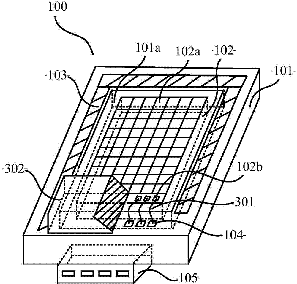
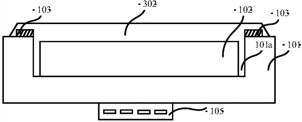
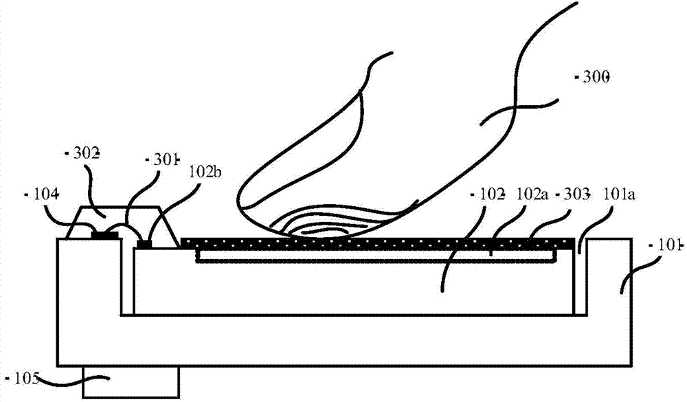
[0063] see Figure 1 to Figure 4 ,in, figure 1 Shown is a schematic structural view of the first embodiment of the packaging structure of the semiconductor capacitive fingerprint sensor of the present invention, wherein the packaging structure includes a planar fingerprint sensor assembly 100 . As shown in the figure, the planar sensor assembly 100 mainly includes a rectangular substrate 101 and a planar sensor die 102. A groove 101a is opened on the front side of the grooved substrate 101, and the length and width of the groove 101a are slightly larger than that of the planar sensor. In the die 102 , the depth of the groove 101 a is slightly higher than the height of the planar sensor die 102 . In this embodiment, the packaging structure can embed the sensor die 102 into the fixed area of ​​the planar sensor die 102 at the bottom of the substrate groove 101a, and make the front surface of the planar sensor die 102 slightly lower than the substrate 101 on the horizontal plane...

Embodiment 2

[0074] Please refer to Figure 5 to Figure 9 ,in, Figure 5 Shown is a schematic structural view of the second embodiment of the package structure of the semiconductor capacitive fingerprint sensor of the present invention, wherein the package structure includes a strip-shaped fingerprint sensor assembly 200 . The strip fingerprint sensor assembly 200 mainly includes the grooved strip substrate 201 and the strip sensor die 202, with interconnection leads (not shown) formed on its front or back and possibly in each layer thereof, the A groove 201 a is formed on the front of the grooved strip substrate 201 . The length and width of the groove 201 a are slightly larger than the strip sensor die 202 , and the groove depth of the groove 201 a is slightly higher than the height of the die 202 . In this embodiment, the strip-shaped sensor die 202 is embedded in the strip-shaped sensor die 202 fixing area at the bottom of the substrate groove 201a, and the front surface of the strip-...


PUM


Abstract

A packaging structure of a semiconductor capacitive fingerprint sensor comprises a semiconductor sensor tube core, a groove type substrate made of insulation materials, a connecting wire, a connector assembly and an injection package structure. The sensor tube core is supported by and fixed at the bottom of a substrate groove through binding agents, the front face or the back face or the side face of the substrate groove is provided with a plurality of multilevel interconnection leads and contact through holes electrically connected between the multilevel interconnection leads, and a connecting welding disc formed by one or more conducting metal edge bars is printed on the grooved face of the substrate. The connecting wire is used for connecting pins of the sensor tube core and the connecting welding disc of the substrate, and the connector assembly is used for enabling the groove type substrate and a printed circuit board to be electrically connected. The connecting welding disc is connected with one or more grounding pins of the connection assembly through the interconnection leads arranged on the front face or the back face of the substrate and located between levels. One or more grounding pins of the connection assembly are electrically connected with the ground plane of the printed circuit board, and the tube core pins, the substrate conducting metal edge bars and the connection wire are packaged through the injection package structure.

Description

technical field [0001] The invention relates to the technical field of integrated circuit packaging, and more specifically, relates to a semiconductor capacitive fingerprint sensor packaging structure. Background technique [0002] In recent years, with the development of fingerprint recognition technology, fingerprint recognition systems are increasingly used in daily life, such as fingerprint recognition access control systems, fingerprint door locks and fingerprint safes, etc., especially for private devices (such as laptops, Tablet PCs, smart phones, Personal Digital Assistant (PDA) devices, fingerprint USBKeys) and other applications for the purpose of verifying a person's identity have become very common. [0003] According to the sensing principle (fingerprint imaging principle and technology), fingerprint sensors can be divided into optical fingerprint sensors, semiconductor capacitive sensors, semiconductor thermal sensors, semiconductor pressure sensors, ultrasonic...

Claims


Application Information

Patent Timeline
IPC IPC(8): G06K9/00
CPCH01L2224/48091H01L2924/00014
Inventor 吴磊
Owner 成都费恩格尔微电子技术有限公司
Why Eureka
Try Eureka