Silicon wafer detection device

A detection device and a technology of silicon wafers, which are applied in the direction of measuring devices, optical testing of flaws/defects, and material analysis through optical means, can solve problems such as inability to display, inability to guarantee the accuracy of silicon wafer detection results, and poor imaging effects. Achieve the effects of ensuring accuracy, improving clarity, and expanding the adjustment range

Pending Publication Date: 2021-12-07
诺德凯(苏州)智能装备有限公司
View PDF0 Cites 0 Cited by
  • Summary
  • Abstract
  • Description
  • Claims
  • Application Information

AI Technical Summary

Problems solved by technology

In the existing technology, the imaging effect of the device used to detect hidden cracks in silicon wafers is poor, and cannot be clearly displayed on the image, and the accuracy of silicon wafer detection results cannot be guaranteed.

Method used


Image

  • Silicon wafer detection device
  • Silicon wafer detection device
  • Silicon wafer detection device

Examples


Embodiment Construction

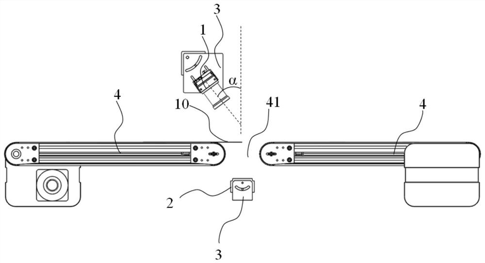
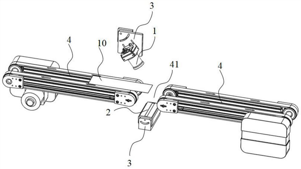
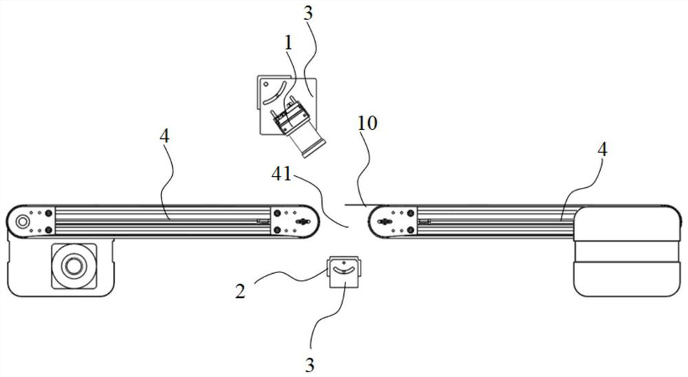
[0033] In order to make the technical problems solved by the present invention, the technical solutions adopted and the technical effects achieved clearer, the technical solutions of the embodiments of the present invention will be further described in detail below in conjunction with the accompanying drawings. Obviously, the described embodiments are only the technical solutions of the present invention. Some, but not all, embodiments. Based on the embodiments of the present invention, all other embodiments obtained by those skilled in the art without making creative efforts belong to the protection scope of the present invention.

[0034] In the description of the present invention, unless otherwise clearly specified and limited, the terms "connected", "connected" and "fixed" should be understood in a broad sense, for example, it can be a fixed connection, a detachable connection, or an integrated ; It can be a mechanical connection or an electrical connection; it can be a d...


PUM


Abstract

The invention relates to the technical field of silicon wafer detection, and discloses a silicon wafer detection device. The silicon wafer detection device comprises a conveying unit, an acquisition part, an infrared light source and adjusting assemblies. The conveying unit is used for conveying silicon wafers in a conveying direction; the acquisition part and the infrared light source are respectively arranged on two sides, perpendicular to the conveying direction, of the conveying unit, and light rays emitted by the infrared light source can penetrate through the silicon wafers and then reach the acquisition end of the acquisition part; the number of the adjusting assemblies is two, the two adjusting assemblies are connected to the acquisition part and the infrared light source respectively, and the adjusting assemblies can adjust the angle of the acquisition part or the infrared light source. According to the invention, the adjustment range of the relative angle between the acquisition part and the infrared light source is expanded, the imaging effect is ensured, the clear degree of defects such as subfissure on the silicon wafers on acquired images is improved, and the accuracy of a detection result is ensured.

Description

technical field [0001] The invention relates to the technical field of silicon wafer detection, in particular to a silicon wafer detection device. Background technique [0002] With the development of science and technology, the rise of the global photovoltaic industry has been brought about. Among them, silicon wafer is one of the important materials in the photovoltaic industry. As the carrier of solar cells, the quality of silicon wafers determines the conversion efficiency of solar cells. Therefore, detecting defects such as cracks on silicon wafers is the key to making solar cells. important link. [0003] With the development of industrial technology, the speed of the silicon wafer production line continues to increase, and manual inspection is limited in speed and cannot keep up with the speed of the production line. Therefore, it is imperative to replace manual inspection with machine vision inspection. High-speed trigger cameras are used to take pictures of silico...

Claims


Application Information

Patent Timeline
Patent Type & Authority Applications(China)
IPC IPC(8): G01N21/88G01N21/89G01N21/84
CPCG01N21/8806G01N21/8851G01N21/8901G01N21/8914G01N21/84G01N2021/8835G01N2021/887G01N2021/8887G01N2021/845
Inventor 卢亚宾曹深深云宏霞张聪梁坤
Owner 诺德凯(苏州)智能装备有限公司
Why Eureka
Try Eureka