Self-luminous display device

a display device and self-luminous technology, applied in the field of self-luminous display devices, can solve the problems of difficult to adequately set either luminance or gradation, the inability to adjust the luminance of organic el elements, and the extremely slight time adjustment, etc., to achieve the effect of adjusting the luminan

Inactive Publication Date: 2006-10-17
JAPAN DISPLAY CENTRAL CO LTD
View PDF4 Cites 34 Cited by
  • Summary
  • Abstract
  • Description
  • Claims
  • Application Information

AI Technical Summary

Benefits of technology

[0014]An object of the present invention is to provide, as a solution to the above problem, a self-luminous display device which can adjust the luminance irrespective of gradation control.

Problems solved by technology

Therefore, the luminance of the organic EL element cannot be adjusted by changing the power-supply voltage.
However, extremely slight time adjustment is required and, as a result, it becomes difficult to adequately set either the luminance or gradation.
However, if the currents flowing through all of the organic EL elements in the luminance adjusting system are equally reduced, the white balance cannot be maintained due to a difference in the luminance characteristics of the organic EL elements which depend on the luminescent colors of red, green and blue.
If a correction circuit which corrects variation amounts of video signal levels for respective luminescent colors is used in order to solve the above problem, it cannot be avoided that the circuit configuration is complicated in comparison with that of the brightness adjusting system of the liquid crystal display device.

Method used


Image

  • Self-luminous display device
  • Self-luminous display device
  • Self-luminous display device

Examples


first embodiment

[0047]There will now be described an organic EL display device according to the present invention with reference to the accompanying drawings.

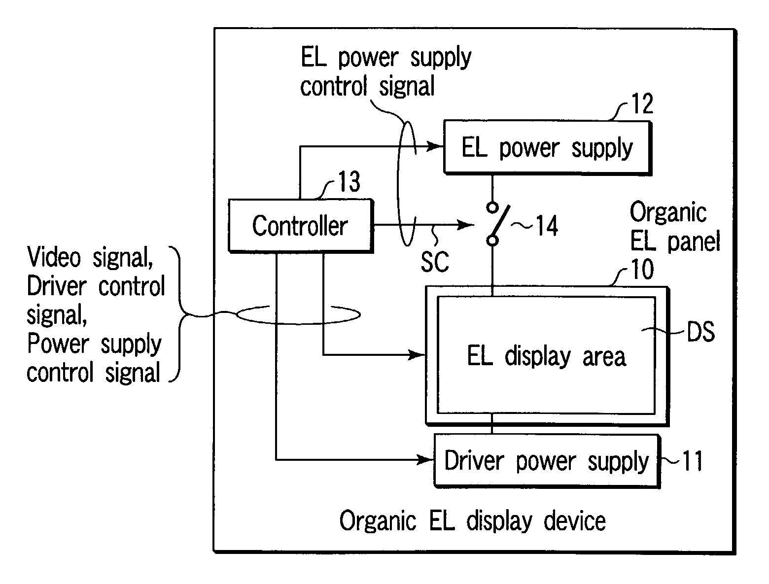
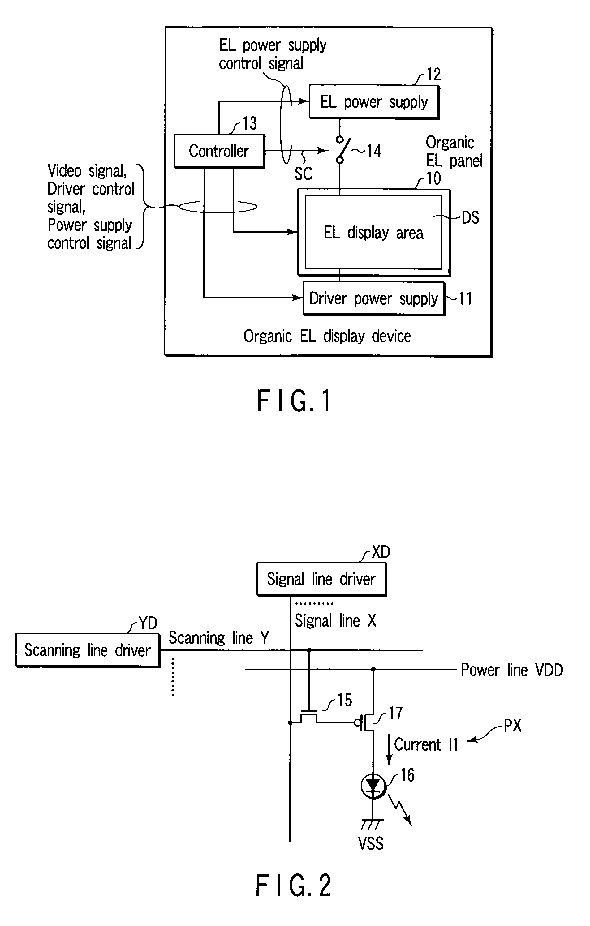
[0048]FIG. 1 shows the whole circuit configuration of the organic EL display device and FIG. 2 shows the circuit configuration of a display pixel PX of the organic EL display device. The organic EL display device includes an organic EL panel 10 which displays an image, a driver power supply 11 which produces a driver power-supply voltage for the organic EL panel 10, an EL power supply 12 which produces an EL power-supply voltage for the organic EL panel 10, and a controller 13 which performs the control operation to operate the organic EL panel 10 in a normal mode and in a still image display mode. The organic EL panel 10 includes a plurality of display pixels PX forming an EL display area DS which serves as a display screen, a plurality of scanning lines Y disposed along respective rows of the display pixels PX, a plurality of signal lines X ...

second embodiment

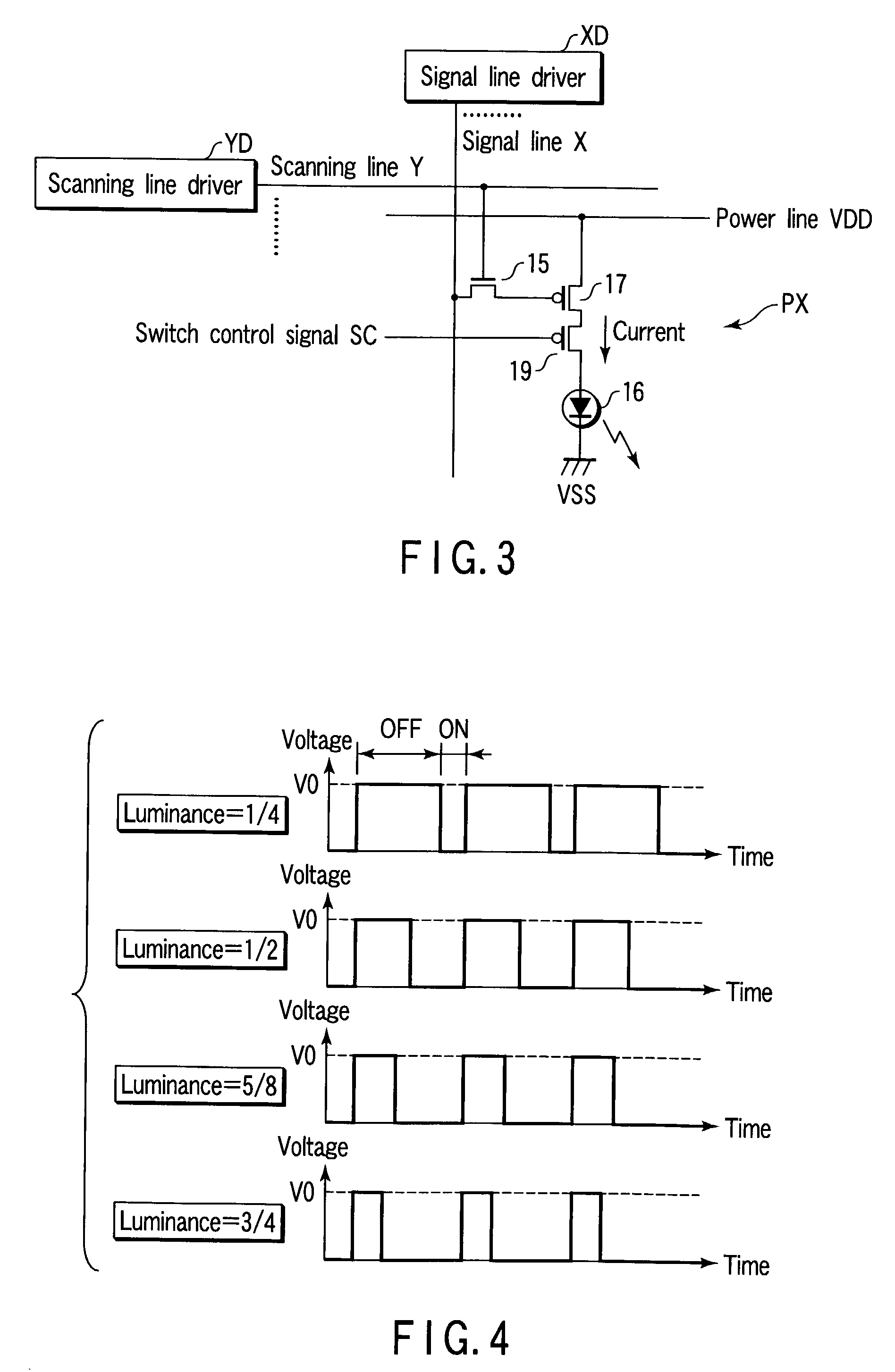
[0055]Next, an organic EL display device according to the present invention is explained. FIG. 3 shows the circuit configuration of a display pixel PX of the organic EL display device. The organic EL display device is similar to the organic EL display device shown in FIG. 1. Therefore, in FIG. 3, portions similar to those of the organic EL display device shown in FIG. 1 are denoted by the same reference symbols. The dimmer switch 14 shown in FIG. 1 is omitted in the present embodiment, but the whole configuration except the above point is the same as the configuration shown in FIG. 1. In the organic EL display device, each display pixel PX has a dimmer switch 19 which is used instead of the dimmer switch 14, as shown in FIG. 3. The dimmer switch 19 is connected in series between an organic EL element 16 and a driving element 17 and controlled by a switch control signal SC from a controller 13. For example, the dimmer switch 19 is formed of a P-channel thin-film transistor like the d...

third embodiment

[0062]Next, an organic EL display device according to the present invention is explained. FIG. 8 schematically shows a luminance adjusting system of a display pixel PX of the organic EL display device, and FIG. 9 shows the circuit configuration of the organic EL panel 10. The organic EL display device is similar to the organic EL display device shown in FIG. 1. Therefore, in FIGS. 8 and 9, portions which are similar to those of the organic EL display device shown in FIG. 1 are denoted by the same reference symbols. The dimmer switch 14 shown in FIG. 1 is omitted in the present embodiment and the remaining configuration is the same as that shown in FIG. 1. In the organic EL display device, a plurality of dimmer switches 22 are provided instead of the dimmer switch 14. As shown in FIG. 8, each dimmer switch 22 is a P-channel thin-film transistor inserted into a power line VDD formed along the display pixels PX of one row on a glass plate which is used as a circuit board of the organic...


PUM


Abstract

An organic EL display device includes display pixels forming a display screen, scanning lines disposed along rows of the display pixels, signal lines disposed along columns of the display pixels, and a power supply section which supplies a power-supply voltage to the display pixels. Each of the display pixels includes a luminous element, a pixel switch which receives a video signal from a corresponding one of the signal lines in response to a scanning signal from a corresponding scanning line and a driving element which is connected between the luminous element and the power supply section to supply a driving current corresponding to the video signal from the pixel switch to the luminous element. Particularly, each luminous element is connected to the power supply section via a dimmer switch portion.

Description

CROSS-REFERENCE TO RELATED APPLICATIONS[0001]This application is based upon and claims the benefit of priority from the prior Japanese Patent Applications No. 2001-304723 filed Sep. 28, 2001; and No. 2001-375002, filed Sep. 29, 2001, the entire contents of both of which are incorporated herein by reference.BACKGROUND OF THE INVENTION[0002]1. Field of the Invention[0003]This invention relates to a display device having a plurality of display pixels arrayed in a matrix form to display an image, to a driving method thereof and, for example, to a self-luminous display device in which each display pixel is configured by a self-luminous element such as an organic EL (Electro Luminescence) element.[0004]2. Description of the Related Art[0005]In recent years, much attention has been focused on organic EL display devices as monitor displays for portable information terminals since the devices have such characteristics as lightness, thinness, and high luminance. A typical organic EL display d...

Claims


Application Information

Patent Timeline
Patent Type & Authority Patents(United States)
IPC IPC(8): G09G3/30G09G3/20G09G3/22G09G3/32
CPCG09G3/3233G09G3/2081G09G3/22G09G2300/0417G09G2300/0842G09G2300/0857G09G2300/0861G09G2300/0866G09G2310/0221G09G2320/0606G09G2320/0626G09G2320/10G09G2330/02G09G2340/0428G09G3/30
Inventor HANARI, JUNMAMETSUKA, KOJIWATANABE, MANABU
Owner JAPAN DISPLAY CENTRAL CO LTD
Why Eureka
Try Eureka