Check patentability & draft patents in minutes with Patsnap Eureka AI!

Pixel structure

A pixel structure and pixel electrode technology, applied in nonlinear optics, instruments, optics, etc., can solve the problems of liquid crystal molecules toppling, dark lines on the display screen, reduced transmittance, etc., and achieve high resolution, uniform and consistent alignment, Substantial effect of alignment

Active Publication Date: 2022-01-07
AU OPTRONICS CORP
View PDF7 Cites 2 Cited by
  • Summary
  • Abstract
  • Description
  • Claims
  • Application Information

AI Technical Summary

Problems solved by technology

However, the electric field at the boundary of different alignment directions will cause the liquid crystal molecules to fall too much to the extension direction at the boundary of different alignment directions due to the excessive fringe electric field effect, so that dark lines will be generated when forming a display screen and the efficiency of liquid crystals will be reduced. In turn, the transmittance is reduced and the display quality is seriously affected.

Method used


Image

  • Pixel structure
  • Pixel structure
  • Pixel structure

Examples


Embodiment Construction

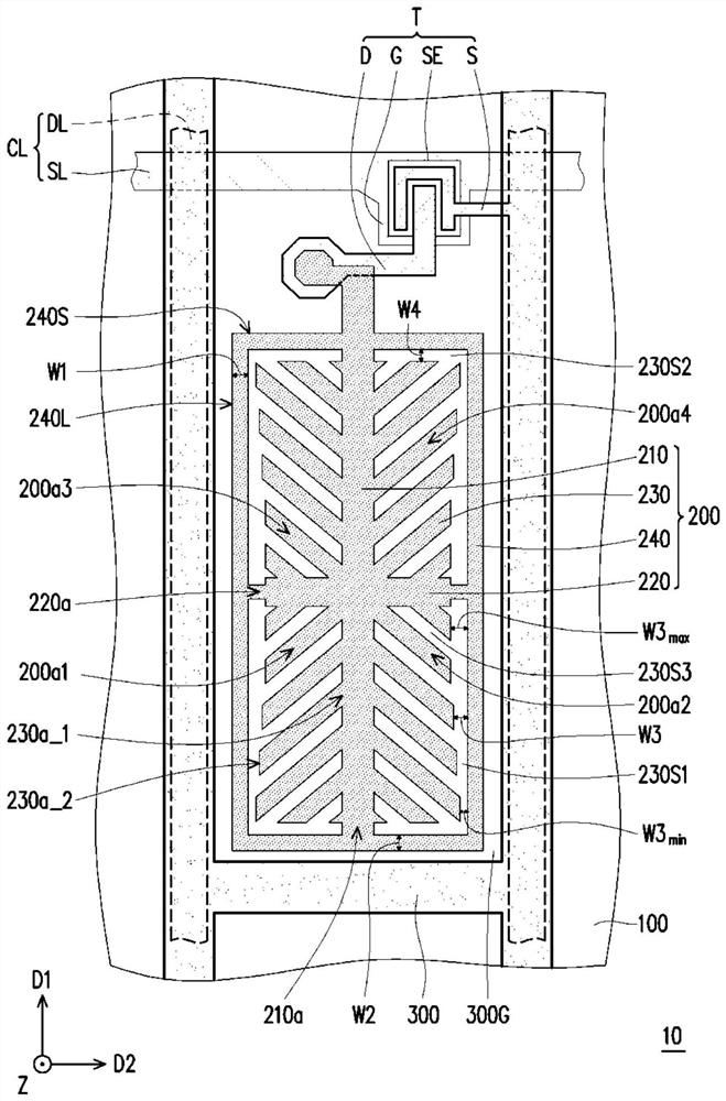
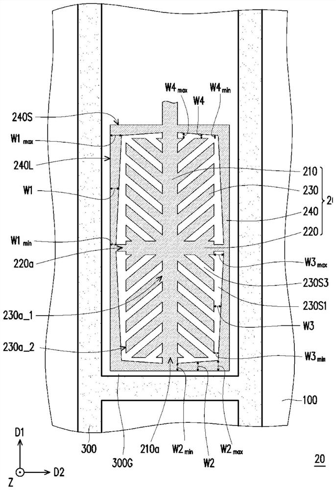
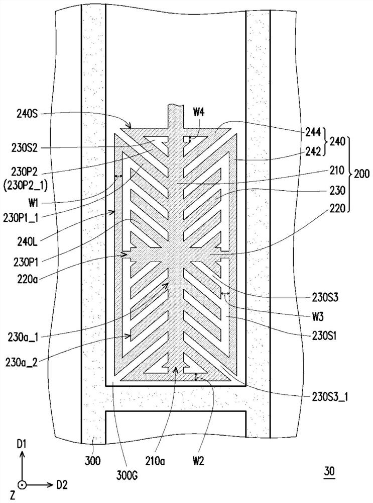
[0067] In the drawings, the thickness of layers, films, panels, regions, etc., are exaggerated for clarity. Throughout the specification, the same reference numerals denote the same elements. It will be understood that when an element such as a layer, film, region, or substrate is referred to as being "on" or "connected to" another element, it can be directly on or connected to the other element, or Intermediate elements may also be present. In contrast, when an element is referred to as being "directly on" or "directly connected to" another element, there are no intervening elements present. As used herein, "connected" may refer to physical and / or electrical connection. Furthermore, "electrically connected" or "coupled" may mean that other elements exist between two elements.

[0068] As used herein, "about," "approximately," or "substantially" includes stated values ​​and averages within acceptable deviations from a particular value as determined by one of ordinary skill ...


PUM


Abstract

The invention discloses a pixel structure which comprises a substrate and a pixel electrode. The pixel electrode is disposed on the substrate. The pixel electrode includes a first main pattern, a second main pattern, a plurality of branch patterns and a peripheral pattern. The first main pattern and the second main pattern are staggered to divide at least four areas, the branch patterns are respectively positioned in the areas, one end of each branch pattern positioned in each area is connected with at least one of the first main pattern and the second main pattern, any two adjacent branch patterns are separated from each other, and the first main pattern and the second main pattern are separated from each other. A plurality of first slits are arranged between the other ends of the branch patterns closest to at least one of the first main pattern and the second main pattern and the peripheral pattern, and the other ends of the rest branch patterns are connected with the peripheral pattern.

Description

[0001] This application is a divisional application. The application number of its parent application is 201811031369.3. The applicant is AU Optronics Co., Ltd. The application date is September 5, 2018. The invention name is pixel structure. technical field [0002] The present invention relates to a semiconductor structure, and in particular to a pixel structure. Background technique [0003] With the rapid development of large-size liquid crystal display panels, the liquid crystal display panels must have wide viewing angle characteristics in order to meet the needs of use. In order to make the liquid crystal display panel have a higher contrast and a wider viewing angle, the pixel electrodes usually include different alignment directions, so that the liquid crystal molecules in different alignment regions will fall in different directions under the applied voltage. However, the electric field at the boundary of different alignment directions will cause the liquid crystal...

Claims


Application Information

Patent Timeline
Patent Type & Authority Applications(China)
IPC IPC(8): G02F1/1343
CPCG02F1/134309
Inventor 龚晏瑩王奕筑郑伟成
Owner AU OPTRONICS CORP
Features
  • R&D
  • Intellectual Property
  • Life Sciences
  • Materials
  • Tech Scout
  • Unparalleled Data Quality
  • Higher Quality Content
  • 60% Fewer Hallucinations
Learn More