
Patsnap Eureka
For R&D, Patsnap Eureka makes reading and utilizing patents & technical documents easy.
Patsnap Eureka AIR
Designed for self-driven R&D workflows. Generate viable solutions, solve complex R&D challenges, empower your innovation with AI.

Patsnap Eureka Materials
Designed for material experts only. Revolutionize your material R&D, from search, analyze, to developing new materials.

TechResearch
Generate reliable direction feasibility study reports for your R&D in just a few steps.

TechSeek
Discover and master advanced knowledge NOW. Basics, ideas, possibilities, all at once.

TechMind
As an expert in R&D Theories, TechMind can generates customized viable solutions instantly.

TechRisk
Analyze your overall solution with one click, know your potential R&D risks in advance.

TechMonitor
Get weekly tech updates, stay abreast of the latest tech innovations and key insights.
Microelectronic devices with lower recessed conductive structures and related methods and systems
A technology of microelectronic devices and conductive structures, used in circuits, electrical components, semiconductor devices, etc.
- Summary
- Abstract
- Description
- Claims
- Application Information
AI Technical Summary
Problems solved by technology
Method used
Image

Examples
Embodiment 1
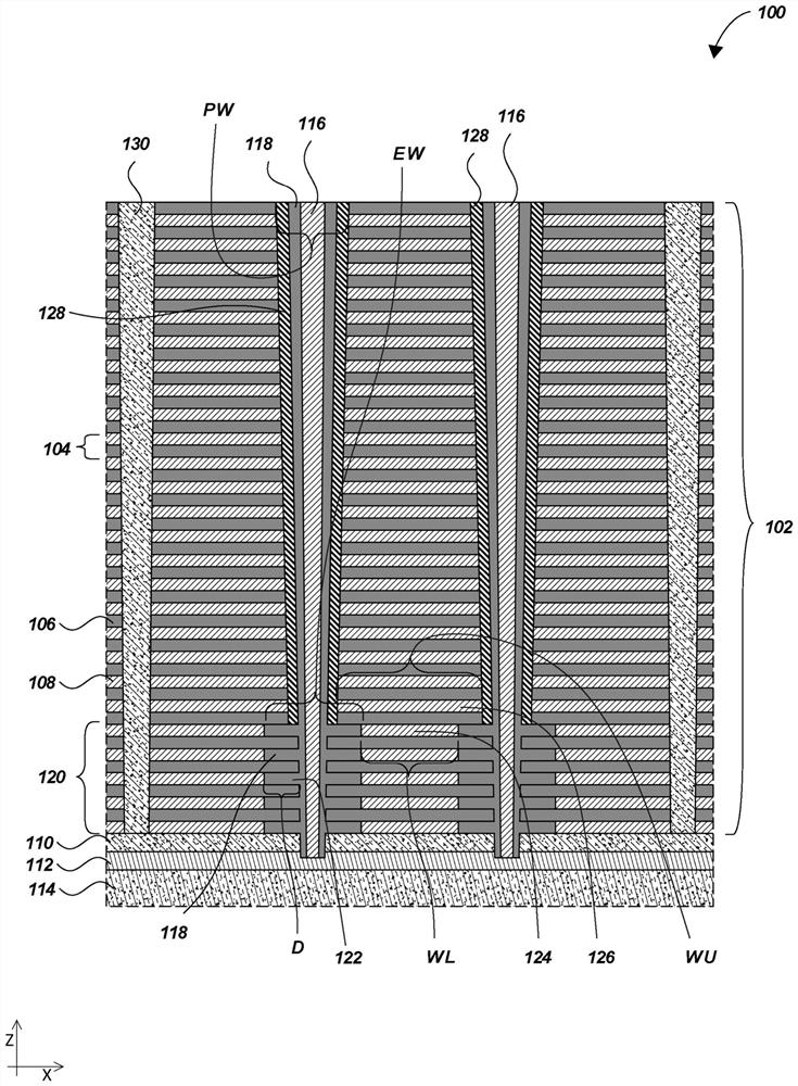
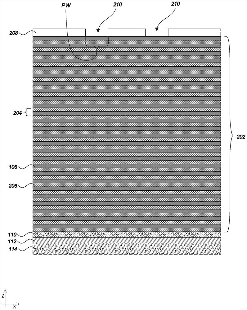
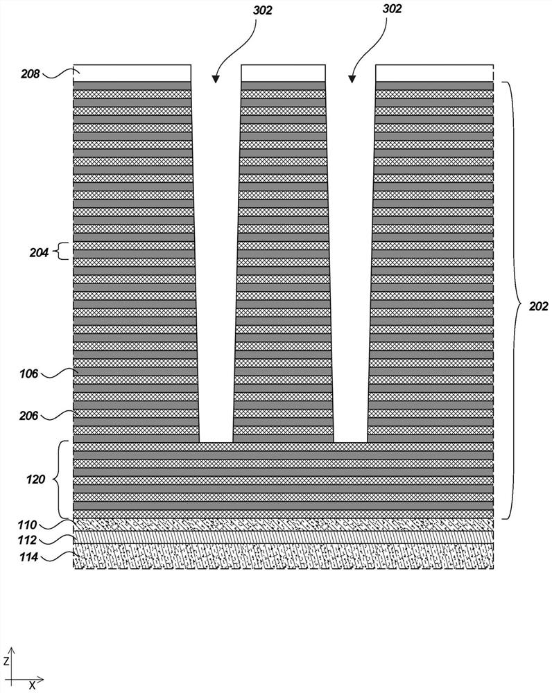
[0115] Embodiment 1: A microelectronic device comprising: a stack structure comprising a vertically alternating sequence of insulating structures and conductive structures arranged in layers; a conductive contact structure extending through the stack structure; and the conductive contact structure and an insulating material between the layers of the stack structure; in the lower portion of the stack structure, one of the plurality of conductive structures has a first width extending between a pair of the conductive contact structures portion; in a portion of the stack structure above the lower layer portion, another conductive structure of the plurality of conductive structures has another portion extending a second width between the pair of conductive contact structures, the first The second width is greater than the first width.
Embodiment 2
[0116] Embodiment 2: The microelectronic device of Embodiment 1, wherein the conductive contact structures taper in width from a widest width at the top of the stack structure to a width at or below the stack structure bottom. The narrowest width.
Embodiment 3
[0117] Embodiment 3: The microelectronic device of any one of embodiments 1 and 2, wherein: the insulating material tapers in width across the portion above the underlying portion of the stack; And the insulating material in the lower portion extends laterally to define an insulating extension vertically adjacent an end of the insulating structure of the lower portion.
PUM
 Abstract
Description
Claims
Application Information
 - R&D Engineer
- R&D Manager
- IP Professional
- Industry Leading Data Capabilities
- Powerful AI technology
- Patent DNA Extraction
Browse by: Latest US Patents, China's latest patents, Technical Efficacy Thesaurus, Application Domain, Technology Topic, Popular Technical Reports.
© 2024 PatSnap. All rights reserved.Legal|Privacy policy|Modern Slavery Act Transparency Statement|Sitemap|About US| Contact US: help@patsnap.com