Pixel structure and exposure method thereof

A technology of pixel structure and exposure method, which is applied in the directions of image communication, color TV parts, TV system parts, etc. problems such as wiring complexity, to achieve the effect of improving fill factor, reducing complexity, and reducing yield risk

Pending Publication Date: 2022-01-18
ONEPLUS TECH SHENZHEN
View PDF6 Cites 0 Cited by
  • Summary
  • Abstract
  • Description
  • Claims
  • Application Information

AI Technical Summary

Problems solved by technology

[0005] In view of this, the present application provides a pixel structure and its exposure method to solve the problem of using different control methods for the pixels in each pixel area to control the exposure of different durations, which increases the complexity of the exposure circuit, and at the same time The complexity of the metal wiring above the pixel is increased, and due to the increase in the complexity of the exposure circuit and metal wiring, the fill factor of the exposure circuit is reduced, and the risk of the yield of the lens module is increased.

Method used


Image

  • Pixel structure and exposure method thereof
  • Pixel structure and exposure method thereof
  • Pixel structure and exposure method thereof

Examples


Embodiment Construction

[0023] The technical solutions in the embodiments of the present application will be clearly and completely described below in conjunction with the accompanying drawings. Apparently, the described embodiments are only some of the embodiments of the present application, not all of them. Based on the embodiments in this application, all other embodiments obtained by those skilled in the art without making creative efforts belong to the scope of protection of this application. In the case of no conflict, the following embodiments and technical features thereof can be combined with each other.

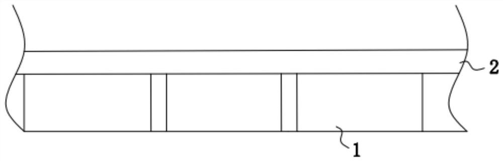
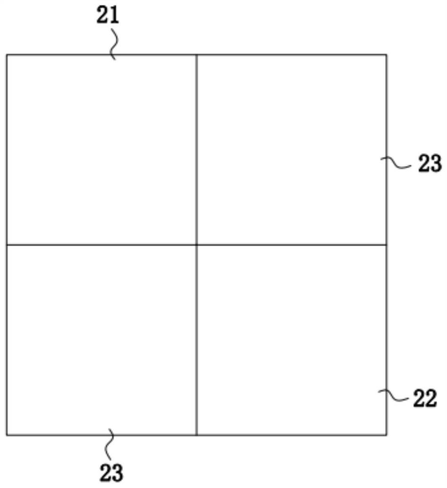
[0024] see figure 1 , the present application provides a lens module, including: a pixel layer 1, an electrochromic layer 2 and a control circuit; The color-changing layer 2 includes a plurality of electrochromic blocks, one electrochromic block covers a type of pixel in the pixel layer 1; the control circuit is electrically connected with the pixel layer and the electrochromic layer 2, a...


PUM


Abstract

The invention discloses a lens module, and the module comprises a pixel layer which comprises at least two kinds of pixels used for collecting light field information of different brightness levels; an electrochromism layer which is arranged on the pixel layer, wherein the electrochromism layer comprises a plurality of electrochromism blocks, one electrochromism block covers one type of pixels of the pixel layer, and the electrochromism layer has the characteristic that a transparent state and a non-transparent state are gradually changed; a control circuit which is electrically connected with the electrochromic layer and the pixel layer, wherein the control circuit is used for controlling the same exposure time of each pixel of the pixel layer and used for controlling the light transmittance of each electrochromic block of the electrochromic layer, and the light transmittance of the electrochromic block corresponding to the pixel with the higher collection brightness level is lower; therefore, the complexity of the exposure circuit is reduced, the complexity of metal wiring above the pixel layer is also reduced, the filling stamp of the exposure circuit is improved, and the yield risk of the lens module is reduced.

Description

technical field [0001] The present application relates to the field of imaging technology, in particular to a pixel structure and its exposure method. Background technique [0002] With the research and development of camera technology, in order to solve the problem of too bright or too dark in high-contrast camera scenes, 3-HDR technology (High Dynamic Range, pixel-level hierarchical exposure technology) is currently used for imaging. [0003] The implementation of 3-HDR technology is to use different exposure times for each sub-pixel in a pixel area, use long-exposure sub-pixels to collect dark-field image information, and use short-exposure sub-pixels to collect bright-field image information. And the sub-pixels with normal exposure time are used to collect the image information of the normal light field, and then combine the image information of the bright field, dark field and normal light field to generate image information with a high dynamic range, which solves the p...

Claims


Application Information

Patent Timeline
Patent Type & Authority Applications(China)
IPC IPC(8): H04N5/235H04N5/225H04N5/351H04N5/355
CPCH04N23/55H04N23/73H04N23/741H04N25/50H04N25/57
Inventor 苏丹丹武广文刘伟肖青刘政王志
Owner ONEPLUS TECH SHENZHEN
Why Eureka
Try Eureka