Press-fit jig and press-fit method for printed circuit board

A printed circuit board and press-fit jig technology, applied in the directions of printed circuit, printed circuit manufacturing, multilayer circuit manufacturing, etc., can solve the problems such as the inability of the PCB to be tightly closed, the unbalanced pressure on the PCB, and the poor pressing effect. Good pressing effect, good force consistency, and the effect of improving air tightness and pressing accuracy

Pending Publication Date: 2022-02-22
东莞市瑞勤电子有限公司
View PDF0 Cites 0 Cited by
  • Summary
  • Abstract
  • Description
  • Claims
  • Application Information

AI Technical Summary

Problems solved by technology

In the existing press-fit operation, several screws around the press-fit fixture act as all the pressure sources, and the PCB board is pressed by the locking screws. Such a design may cause the entire PCB to appear larger in the area where no screws are locked. Unclosed area, poor pressing effect and low yield
In addition, in t

Method used


Image

  • Press-fit jig and press-fit method for printed circuit board
  • Press-fit jig and press-fit method for printed circuit board
  • Press-fit jig and press-fit method for printed circuit board

Examples


Example Embodiment

[0031] Various embodiments of the present invention will be described in more detail below with reference to the accompanying drawings. In each of the drawings, the same components are expressed by the same or similar reference numerals. For the sake of clarity, the various parts in the drawings are not drawn. In addition, some well-known portions may not be shown in the figure.

[0032] DETAILED DESCRIPTION OF THE PREFERRED EMBODIMENTS Many of the specific details of the present invention, such as structural, material, size, processing, and techniques of the components are described below, in order to understand the present invention more clearly. However, as will be appreciated by those skilled in the art, the present invention may be implemented without follow these specific details.

[0033] It should be understood that when the structure of the component is described, when one layer, one area is referred to as at another layer, another area "above" or "above", it may refer to...


PUM


Abstract

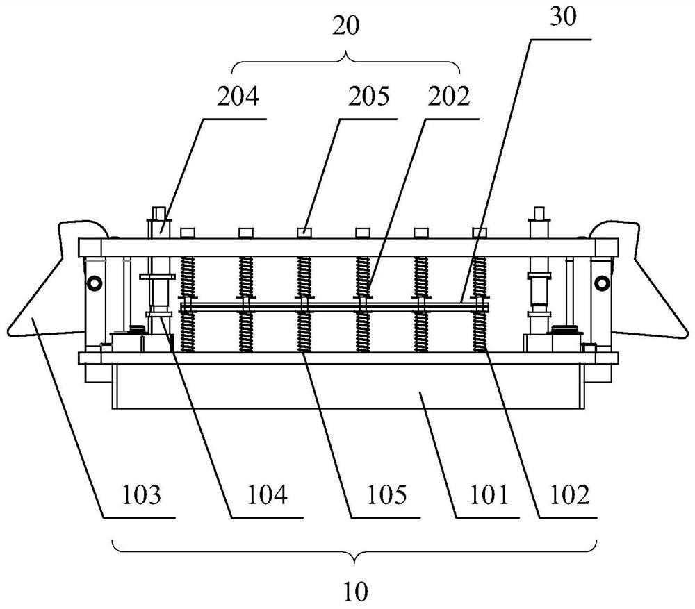
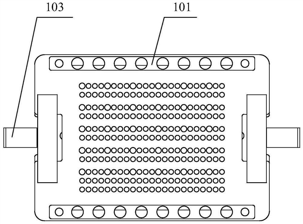
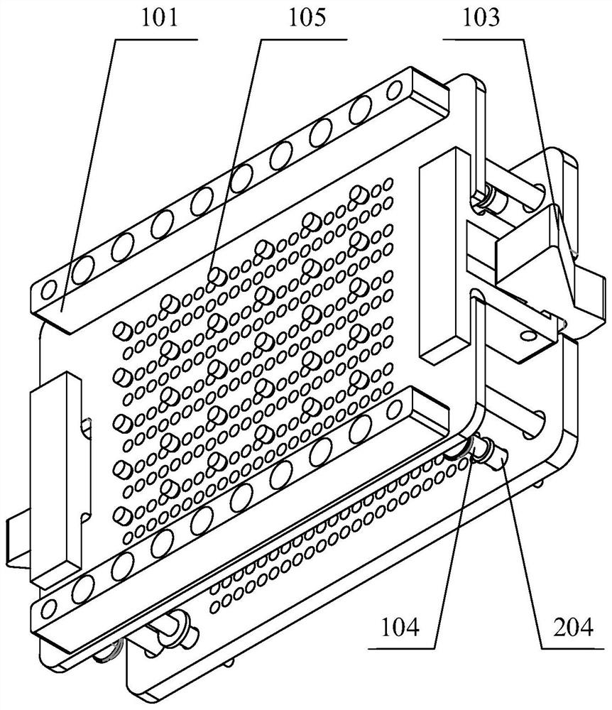
The invention discloses a press-fit jig and a press-fit method for a printed circuit board. According to the embodiment of the invention, the press-fit jig for a printed circuit board comprises a bottom plate which is used for placing a printed circuit board; and a cover plate which is matched with the bottom plate and is used for covering the printed circuit board. The bottom plate is provided with a first press-fit column located on the bottom plate, and a first spring located on the first press-fit column. The cover plate is provided with a second press-fit column located on the cover plate, and a second spring located on the second press-fit column. The first spring and/or the second spring are/is deformed by locking the bottom plate and the cover plate. The deformed first spring and/or the deformed second spring provide press-fit force for the printed circuit board so as to press the printed circuit board. According to the press-fit jig and the press-fit method for the printed circuit board, spring press fit is adopted, the stress consistency is better, press fit is uniform, the air tightness after press fit is good, the precision is high, and the product yield is high.

Description

technical field [0001] The invention relates to the technical field of micro-electromechanical system manufacturing, in particular to a pressing fixture and a pressing method for printed circuit boards. Background technique [0002] Micro-Electro-Mechanical Systems (MEMS, Micro-Electro-Mechanical System), also known as micro-electro-mechanical systems, micro-systems, micro-machines, etc., refers to high-tech devices with a size of a few millimeters or even smaller. During the manufacturing process of products including MEMS, the pressing of printed circuit boards is often involved. [0003] In the prior art, during the production process of a stacked MEMS microphone with a multi-layer PCB (Printed Circuit Board, printed circuit board), the multi-layer PCB needs to be pressed together. In the existing press-fit operation, several screws around the press-fit fixture act as all the pressure sources, and the PCB board is pressed by the locking screws. Such a design may cause th...

Claims


Application Information

Patent Timeline
IPC IPC(8): H05K3/46
CPCH05K3/4611H05K3/4638H05K2203/068
Inventor 王松陈为波
Owner 东莞市瑞勤电子有限公司
Why Eureka
Try Eureka